
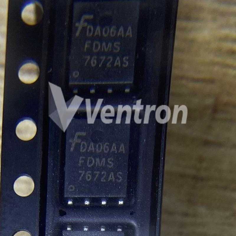
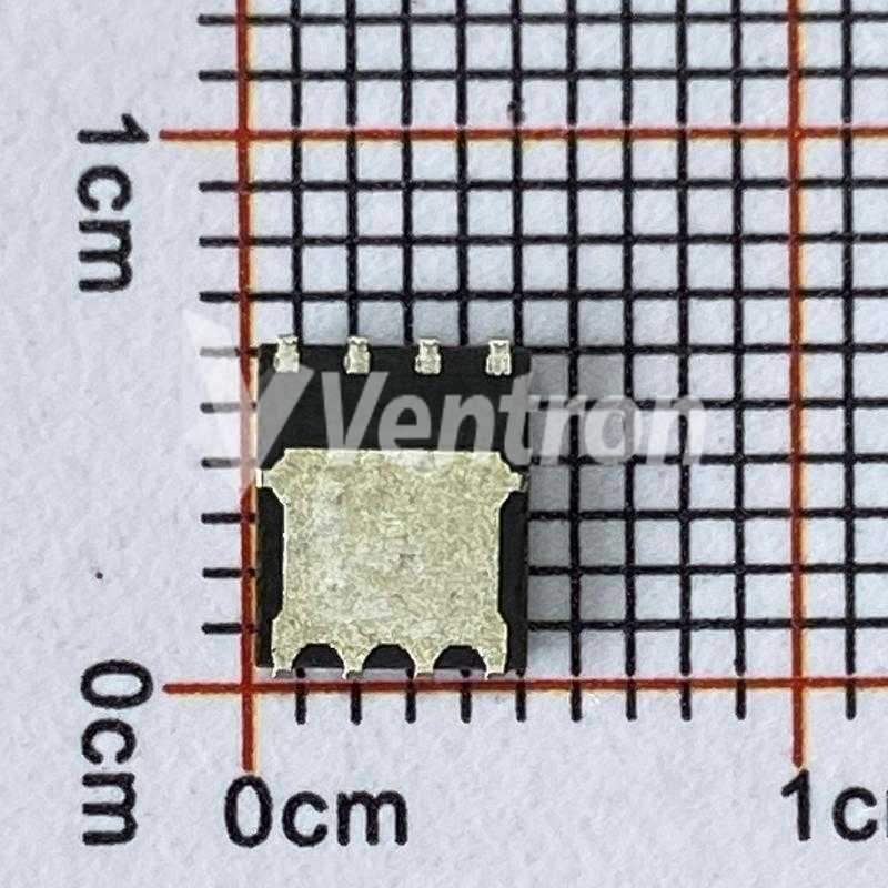
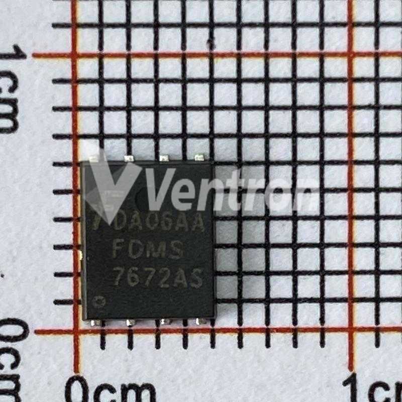
Fairchild/ON Semiconductor FDMS7672AS
- Part Number:
- FDMS7672AS
- Manufacturer:
- Fairchild/ON Semiconductor
- Ventron No:
- 2849849-FDMS7672AS
- Description:
- MOSFET N-CH 30V SYNCFET POWER56
- ECAD Model:
-
- Datasheet:
- FDMS7672AS


Fairchild/ON Semiconductor FDMS7672AS technical specifications, attributes, parameters and parts with similar specifications to Fairchild/ON Semiconductor FDMS7672AS.
- Lifecycle StatusACTIVE (Last Updated: 3 days ago)
- Factory Lead Time18 Weeks
- MountSurface Mount
- Mounting TypeSurface Mount
- Package / Case8-PowerTDFN
- Number of Pins8
- Weight68.1mg
- Transistor Element MaterialSILICON
- Operating Temperature-55°C~150°C TJ
- PackagingTape & Reel (TR)
- SeriesPowerTrench®, SyncFET™
- JESD-609 Codee3
- Pbfree Codeyes
- Part StatusActive
- Moisture Sensitivity Level (MSL)1 (Unlimited)
- Number of Terminations5
- ECCN CodeEAR99
- Resistance3.5MOhm
- Terminal FinishTin (Sn)
- SubcategoryFET General Purpose Power
- TechnologyMOSFET (Metal Oxide)
- Terminal PositionDUAL
- JESD-30 CodeR-XDSO-N5
- Number of Elements1
- Power Dissipation-Max2.5W Ta 46W Tc
- Element ConfigurationSingle
- Operating ModeENHANCEMENT MODE
- Power Dissipation45W
- Case ConnectionDRAIN
- Turn On Delay Time12 ns
- FET TypeN-Channel
- Transistor ApplicationSWITCHING
- Rds On (Max) @ Id, Vgs4m Ω @ 18A, 10V
- Vgs(th) (Max) @ Id3V @ 1mA
- Input Capacitance (Ciss) (Max) @ Vds2820pF @ 15V
- Current - Continuous Drain (Id) @ 25°C19A Ta 42A Tc
- Gate Charge (Qg) (Max) @ Vgs46nC @ 10V
- Rise Time5ns
- Drive Voltage (Max Rds On,Min Rds On)4.5V 10V
- Vgs (Max)±20V
- Fall Time (Typ)4 ns
- Turn-Off Delay Time28 ns
- Continuous Drain Current (ID)42A
- Gate to Source Voltage (Vgs)20V
- Drain to Source Breakdown Voltage30V
- Pulsed Drain Current-Max (IDM)90A
- Avalanche Energy Rating (Eas)60 mJ
- Nominal Vgs1.9 V
- Height1.05mm
- Length5mm
- Width6mm
- REACH SVHCNo SVHC
- Radiation HardeningNo
- RoHS StatusROHS3 Compliant
- Lead FreeLead Free
FDMS7672AS Description
The FDMS7672AS was created with the goal of reducing power conversion losses. The lowest RDS(on) while maintaining great switching performance has been achieved by combining advances in both semiconductor and packaging technology. This device also has a monolithic Schottky body diode, which is very efficient.
FDMS7672AS Features 100% UIL tested
RoHS Compliant
MSL1 robust package design
SyncFET Schottky Body Diode
Max rDS(on) = 4.0 mΩ at VGS = 10 V, ID = 18 A
Max rDS(on) = 4.5 mΩ at VGS = 7 V, ID = 16 A
Advanced Package and Silicon combination for low rDS(on) and high efficiency
FDMS7672AS Applications
Telecom secondary side rectification
Notebook Vcore/GPU low-side switch
Networking Point of Load low-side switch
Synchronous Rectifier for DC/DC Converters
FDMS7672AS More Descriptions
Trans MOSFET N-CH Si 30V 19A 8-Pin PQFN EP T/R
The FDMS7672AS has been designed to minimize losses in power conversion application. Advancements in both silicon and package technologies have been combined to offer the lowest rDS(on) while maintaining excellent switching performance. This device has the added benefit of an efficient monolithic Schottky body diode.
MOSFET, N CH, 30V, 42A, POWER56; Transistor Polarity:N Channel; Continuous Drain Current Id:42A; Drain Source Voltage Vds:30V; On Resistance Rds(on):0.0032ohm; Rds(on) Test Voltage Vgs:10V; Threshold Voltage Vgs Typ:1.9V; Power Dissipation Pd:46W; Operating Temperature Range:-55°C to 150°C; Transistor Case Style:Power 56; No. of Pins:8; MSL:MSL 1 - Unlimited; SVHC:No SVHC (19-Dec-2012)
The three parts on the right have similar specifications to FDMS7672AS.
-
ImagePart NumberManufacturerLifecycle StatusFactory Lead TimeMountMounting TypePackage / CaseNumber of PinsWeightTransistor Element MaterialOperating TemperaturePackagingSeriesJESD-609 CodePbfree CodePart StatusMoisture Sensitivity Level (MSL)Number of TerminationsECCN CodeResistanceTerminal FinishSubcategoryTechnologyTerminal PositionJESD-30 CodeNumber of ElementsPower Dissipation-MaxElement ConfigurationOperating ModePower DissipationCase ConnectionTurn On Delay TimeFET TypeTransistor ApplicationRds On (Max) @ Id, VgsVgs(th) (Max) @ IdInput Capacitance (Ciss) (Max) @ VdsCurrent - Continuous Drain (Id) @ 25°CGate Charge (Qg) (Max) @ VgsRise TimeDrive Voltage (Max Rds On,Min Rds On)Vgs (Max)Fall Time (Typ)Turn-Off Delay TimeContinuous Drain Current (ID)Gate to Source Voltage (Vgs)Drain to Source Breakdown VoltagePulsed Drain Current-Max (IDM)Avalanche Energy Rating (Eas)Nominal VgsHeightLengthWidthREACH SVHCRadiation HardeningRoHS StatusLead FreePeak Reflow Temperature (Cel)Reach Compliance CodeTime@Peak Reflow Temperature-Max (s)Drain to Source Voltage (Vdss)PublishedTerminal FormThreshold VoltageJEDEC-95 CodeFET FeatureView Compare
-
 FDMS7672ASACTIVE (Last Updated: 3 days ago)18 WeeksSurface MountSurface Mount8-PowerTDFN868.1mgSILICON-55°C~150°C TJTape & Reel (TR)PowerTrench®, SyncFET™e3yesActive1 (Unlimited)5EAR993.5MOhmTin (Sn)FET General Purpose PowerMOSFET (Metal Oxide)DUALR-XDSO-N512.5W Ta 46W TcSingleENHANCEMENT MODE45WDRAIN12 nsN-ChannelSWITCHING4m Ω @ 18A, 10V3V @ 1mA2820pF @ 15V19A Ta 42A Tc46nC @ 10V5ns4.5V 10V±20V4 ns28 ns42A20V30V90A60 mJ1.9 V1.05mm5mm6mmNo SVHCNoROHS3 CompliantLead Free----------
 -
ACTIVE (Last Updated: 1 week ago)12 WeeksSurface MountSurface Mount8-PowerTDFN856.5mg--55°C~175°C TJTape & Reel (TR)PowerTrench®e3yesActive1 (Unlimited)-EAR99-Tin (Sn)-MOSFET (Metal Oxide)---3.33W Ta 125W TcSingle----N-Channel-0.85m Ω @ 47A, 10V3V @ 250μA16590pF @ 20V49A Ta 300A Tc219nC @ 10V-4.5V 10V±20V--300A----------ROHS3 Compliant-260not_compliantNOT SPECIFIED40V-----
-
LAST SHIPMENTS (Last Updated: 1 week ago)-Surface MountSurface Mount8-PowerTDFN890mgSILICON-55°C~150°C TJDigi-Reel®PowerTrench®, SyncFET™e3yesObsolete1 (Unlimited)5EAR99-Tin (Sn)FET General Purpose PowerMOSFET (Metal Oxide)DUALR-PDSO-F513.3W Ta 59W TcSingleENHANCEMENT MODE59WDRAIN11 nsN-ChannelSWITCHING2.8m Ω @ 28A, 10V2.2V @ 1mA2825pF @ 13V28A Ta 60A Tc42nC @ 10V4ns4.5V 10V±12V3 ns33 ns60A12V25V100A45 mJ----No SVHCNoRoHS Compliant-----2017FLAT1.5VMO-240AASchottky Diode (Body)
-
ACTIVE, NOT REC (Last Updated: 2 days ago)6 WeeksSurface MountSurface Mount8-PowerTDFN856.5mg--55°C~175°C TJTape & Reel (TR)PowerTrench®e3yesNot For New Designs1 (Unlimited)-EAR99-Tin (Sn)-MOSFET (Metal Oxide)---3.3W Ta 180W TcSingle----N-Channel-0.65m Ω @ 55A, 10V3V @ 750μA22610pF @ 15V55A Ta 423A Tc285nC @ 10V-4.5V 10V±20V--423A----------ROHS3 CompliantLead Free260not_compliantNOT SPECIFIED30V2017----
Popular Search Part Number
Related Keywords
Search Tags
Latest News
-
25 October 2023
What Is MB10S Bridge Rectifier?
Ⅰ. What is a bridge rectifier?Ⅱ. Overview of MB10S bridge rectifierⅢ. Symbol, footprint and pin configuration of MB10S bridge rectifierⅣ. Technical parameters of MB10S bridge rectifierⅤ. Features of... -
26 October 2023
L293DNE Quadruple Half-H Driver: Symbol, Features, Advantages and More
Ⅰ. Overview of L293DNE quadruple half-H driverⅡ. L293DNE symbol, footprint and pin configurationⅢ. Technical parameters of L293DNE/aⅣ. What are the features of L293DNE?Ⅴ. Working principle of L293DNEⅥ. What... -
26 October 2023
TL494CN PWM Controller: Pin Configuration, Layout Guidelines and Working Principle
Ⅰ. Overview of TL494CN PWM controllerⅡ. Symbol, footprint and pin configuration of TL494CN PWM controllerⅢ. Technical parameters of TL494CN PWM controllerⅣ. What are the features of TL494CN PWM... -
27 October 2023
CD4511BE Decoder: Pin Configuration, Features, Circuit and Applications
Ⅰ. What is a decoder?Ⅱ. Overview of CD4511BE decoderⅢ. Symbol, footprint and pin configuration of CD4511BE decoderⅣ. Technical parameters of CD4511BE decoderⅤ. What are the features of CD4511BE...
Help you to save your cost and time.
Reliable package for your goods.
Fast Reliable Delivery to save time.
Quality premium after-sale service.