Vishay Siliconix IRLR024TR
- Part Number:
- IRLR024TR
- Manufacturer:
- Vishay Siliconix
- Ventron No:
- 2850828-IRLR024TR
- Description:
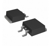
- MOSFET N-CH 60V 14A DPAK
- ECAD Model:
-
- Datasheet:
- IRLR024TR


Vishay Siliconix IRLR024TR technical specifications, attributes, parameters and parts with similar specifications to Vishay Siliconix IRLR024TR.
- Factory Lead Time21 Weeks
- MountSurface Mount
- Mounting TypeSurface Mount
- Package / CaseTO-252-3, DPak (2 Leads Tab), SC-63
- Number of Pins2
- Supplier Device PackageD-Pak
- Operating Temperature-55°C~150°C TJ
- PackagingTape & Reel (TR)
- Published2016
- Part StatusActive
- Moisture Sensitivity Level (MSL)1 (Unlimited)
- Max Operating Temperature150°C
- Min Operating Temperature-55°C
- Voltage - Rated DC60V
- TechnologyMOSFET (Metal Oxide)
- Current Rating14A
- Power Dissipation-Max2.5W Ta 42W Tc
- Element ConfigurationSingle
- Power Dissipation2.5W
- Turn On Delay Time11 ns
- FET TypeN-Channel
- Rds On (Max) @ Id, Vgs100mOhm @ 8.4A, 5V
- Vgs(th) (Max) @ Id2V @ 250μA
- Input Capacitance (Ciss) (Max) @ Vds870pF @ 25V
- Current - Continuous Drain (Id) @ 25°C14A Tc
- Gate Charge (Qg) (Max) @ Vgs18nC @ 5V
- Rise Time110ns
- Drain to Source Voltage (Vdss)60V
- Drive Voltage (Max Rds On,Min Rds On)4V 5V
- Vgs (Max)±10V
- Fall Time (Typ)41 ns
- Turn-Off Delay Time23 ns
- Continuous Drain Current (ID)14A
- Gate to Source Voltage (Vgs)10V
- Drain to Source Breakdown Voltage60V
- Input Capacitance870pF
- Drain to Source Resistance100mOhm
- Rds On Max100 mΩ
- Radiation HardeningNo
- RoHS StatusNon-RoHS Compliant
- Lead FreeContains Lead
IRLR024TR Overview
As an op amp's input capacitance parameter, CI, is defined as the capacitance between the input terminals when one input is grounded, this device's maximum input capacitance is 870pF @ 25V.This device conducts a continuous drain current (ID) of 14A, which is the maximum continuous current transistor can conduct.Using VGS=60V and a specified value of ID, the drain-source breakdown voltage is VDS at which a specified value of ID flows. This device has a drain-source breakdown voltage of 60V (that is, no charge flow from drain to source).When the device is turned off, a turn-off delay time of 23 ns occurs as the input capacitance charges before drain current conduction commences.When a specific gate-to-source voltage (VGS) is applied to bias a MOSFET to the on state, the drain to source resistance is 100mOhm, which means the device is not biased.Before drain current conduction can begin, the device's turning-on delay time takes time to charge its input capacitance. This delay time is 11 ns.Voltage at the gate-source terminal of a FET transistor, called the gate-source voltage, or VGS, can be 10V.This transistor requires a drain-source voltage (Vdss) of 60V.In order to reduce power consumption, this device uses a drive voltage of 4V 5V volts (4V 5V).
IRLR024TR Features
a continuous drain current (ID) of 14A
a drain-to-source breakdown voltage of 60V voltage
the turn-off delay time is 23 ns
single MOSFETs transistor is 100mOhm
a 60V drain to source voltage (Vdss)
IRLR024TR Applications
There are a lot of Vishay Siliconix
IRLR024TR applications of single MOSFETs transistors.
Motor drives and Uninterruptible Power Supplies
Micro Solar Inverter
DC/DC converters
Power Tools
Motor Drives and Uninterruptible Power Supples
Synchronous Rectification
Battery Protection Circuit
Telecom 1 Sever Power Supplies
Industrial Power Supplies
PFC stages, hard switching PWM stages and resonant switching
IRLR024TR More Descriptions
Trans MOSFET N-CH 60V 14A 3-Pin (2 Tab) DPAK T/R
LOGIC MOSFET N-CHANNEL 60V
LOGIC MOSFET N-CHANNEL 60V
The three parts on the right have similar specifications to IRLR024TR.
-
ImagePart NumberManufacturerFactory Lead TimeMountMounting TypePackage / CaseNumber of PinsSupplier Device PackageOperating TemperaturePackagingPublishedPart StatusMoisture Sensitivity Level (MSL)Max Operating TemperatureMin Operating TemperatureVoltage - Rated DCTechnologyCurrent RatingPower Dissipation-MaxElement ConfigurationPower DissipationTurn On Delay TimeFET TypeRds On (Max) @ Id, VgsVgs(th) (Max) @ IdInput Capacitance (Ciss) (Max) @ VdsCurrent - Continuous Drain (Id) @ 25°CGate Charge (Qg) (Max) @ VgsRise TimeDrain to Source Voltage (Vdss)Drive Voltage (Max Rds On,Min Rds On)Vgs (Max)Fall Time (Typ)Turn-Off Delay TimeContinuous Drain Current (ID)Gate to Source Voltage (Vgs)Drain to Source Breakdown VoltageInput CapacitanceDrain to Source ResistanceRds On MaxRadiation HardeningRoHS StatusLead FreeSeriesSurface MountTransistor Element MaterialJESD-609 CodePbfree CodeNumber of TerminationsTerminal FinishTerminal PositionTerminal FormPeak Reflow Temperature (Cel)Reach Compliance CodeTime@Peak Reflow Temperature-Max (s)Pin CountJESD-30 CodeQualification StatusNumber of ElementsConfigurationOperating ModeCase ConnectionTransistor ApplicationDrain Current-Max (Abs) (ID)Drain-source On Resistance-MaxPulsed Drain Current-Max (IDM)DS Breakdown Voltage-MinAvalanche Energy Rating (Eas)View Compare
-
 IRLR024TR21 WeeksSurface MountSurface MountTO-252-3, DPak (2 Leads Tab), SC-632D-Pak-55°C~150°C TJTape & Reel (TR)2016Active1 (Unlimited)150°C-55°C60VMOSFET (Metal Oxide)14A2.5W Ta 42W TcSingle2.5W11 nsN-Channel100mOhm @ 8.4A, 5V2V @ 250μA870pF @ 25V14A Tc18nC @ 5V110ns60V4V 5V±10V41 ns23 ns14A10V60V870pF100mOhm100 mΩNoNon-RoHS CompliantContains Lead--------------------------
 -
--Surface MountTO-252-3, DPak (2 Leads Tab), SC-63-D-Pak-55°C~175°C TJTape & Reel (TR)1998Obsolete1 (Unlimited)---MOSFET (Metal Oxide)-107W Tc---N-Channel19mOhm @ 33A, 10V1V @ 250μA1600pF @ 25V55A Tc50nC @ 4.5V-30V4.5V 10V±16V---------Non-RoHS Compliant-HEXFET®------------------------
-
-Surface MountSurface MountTO-252-3, DPak (2 Leads Tab), SC-63-D-Pak-55°C~150°C TJTape & Reel (TR)1997Active1 (Unlimited)---MOSFET (Metal Oxide)-2.5W Ta 42W Tc---N-Channel100mOhm @ 8.4A, 5V2V @ 250μA870pF @ 25V14A Tc18nC @ 5V-60V4V 5V±10V--14A--870pF-100 mΩ-Non-RoHS Compliant--------------------------
-
--Surface MountTO-252-3, DPak (2 Leads Tab), SC-63---55°C~150°C TJTape & Reel (TR)-Obsolete1 (Unlimited)---MOSFET (Metal Oxide)-2.5W Ta 46W Tc---N-Channel120m Ω @ 6.5A, 5V2V @ 250μA755pF @ 25V13A Tc24nC @ 5V-100V5V±20V---------ROHS3 Compliant--YESSILICONe3yes2MATTE TINSINGLEGULL WINGNOT SPECIFIEDunknownNOT SPECIFIED3R-PSSO-G2COMMERCIAL1SINGLE WITH BUILT-IN DIODEENHANCEMENT MODEDRAINSWITCHING13A0.12Ohm45A100V225 mJ
Popular Search Part Number
Related Keywords
Search Tags
Latest News
-
01 April 2024
M24C16-RMN6TP Structure, Advantages, Package and Other Details
Ⅰ. M24C16-RMN6TP descriptionⅡ. Basic structure and working principle of M24C16-RMN6TPⅢ. Technical parameters of M24C16-RMN6TPⅣ. What are the market competitive advantages of M24C16-RMN6TP?Ⅴ. Package of M24C16-RMN6TPⅥ. Data transmission process... -
02 April 2024
TPS54202DDCR Alternatives, Characteristics, Layout and TPS54202DDCR vs TPS54202DDCT
Ⅰ. What is TPS54202DDCR?Ⅱ. Functional modes of TPS54202DDCRⅢ. Characteristics of TPS54202DDCRⅣ. How to reduce the noise of TPS54202DDCR?Ⅴ. Comparison between TPS54202DDCR and TPS54202DDCTⅥ. Layout of TPS54202DDCRⅦ. How to... -
02 April 2024
L6599D Working Principle, Application, Common Faults and Solutions
Ⅰ. Overview of L6599DⅡ. Line sensing function of L6599DⅢ. Working principle of L6599DⅣ. Application of L6599DⅤ. Application circuit of L6599DⅥ. Common faults and solutions of L6599DⅦ. Typical electrical... -
03 April 2024
ADUM1201BRZ-RL7 Alternatives, Specifications, Application and More
Ⅰ. Overview of ADUM1201BRZ-RL7Ⅱ. Specifications of ADUM1201BRZ-RL7Ⅲ. Propagation delay-related parametersⅣ. Application of ADUM1201BRZ-RL7Ⅴ. How to evaluate the performance of ADUM1201BRZ-RL7?Ⅵ. Functional block diagram of ADUM1201BRZ-RL7Ⅶ. PCB layout of...
Help you to save your cost and time.
Reliable package for your goods.
Fast Reliable Delivery to save time.
Quality premium after-sale service.