Vishay Siliconix IRFR9220
- Part Number:
- IRFR9220
- Manufacturer:
- Vishay Siliconix
- Ventron No:
- 3071491-IRFR9220
- Description:
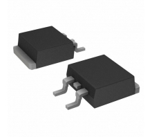
- MOSFET P-CH 200V 3.6A DPAK
- ECAD Model:
-
- Datasheet:
- IRFR9220
Vishay Siliconix IRFR9220 technical specifications, attributes, parameters and parts with similar specifications to Vishay Siliconix IRFR9220.
- MountSurface Mount
- Mounting TypeSurface Mount
- Package / CaseTO-252-3, DPak (2 Leads Tab), SC-63
- Number of Pins3
- Supplier Device PackageD-Pak
- Weight1.437803g
- Operating Temperature-55°C~150°C TJ
- PackagingTube
- Published2015
- Part StatusObsolete
- Moisture Sensitivity Level (MSL)1 (Unlimited)
- Max Operating Temperature150°C
- Min Operating Temperature-55°C
- TechnologyMOSFET (Metal Oxide)
- Number of Elements1
- Number of Channels1
- Power Dissipation-Max2.5W Ta 42W Tc
- Element ConfigurationSingle
- Power Dissipation2.5W
- Turn On Delay Time8.8 ns
- FET TypeP-Channel
- Rds On (Max) @ Id, Vgs1.5Ohm @ 2.2A, 10V
- Vgs(th) (Max) @ Id4V @ 250μA
- Input Capacitance (Ciss) (Max) @ Vds340pF @ 25V
- Current - Continuous Drain (Id) @ 25°C3.6A Tc
- Gate Charge (Qg) (Max) @ Vgs20nC @ 10V
- Rise Time27ns
- Drain to Source Voltage (Vdss)200V
- Drive Voltage (Max Rds On,Min Rds On)10V
- Vgs (Max)±20V
- Fall Time (Typ)19 ns
- Turn-Off Delay Time7.3 ns
- Continuous Drain Current (ID)3.6A
- Gate to Source Voltage (Vgs)20V
- Drain to Source Breakdown Voltage-200V
- Input Capacitance340pF
- Drain to Source Resistance1.5Ohm
- Rds On Max1.5 Ω
- Height2.39mm
- Length6.73mm
- Width6.22mm
- RoHS StatusNon-RoHS Compliant
IRFR9220 Overview
An op amp's input capacitance is defined as the capacitance between both of its input terminals with either input grounded, and 340pF @ 25V is its maximum input capacitance.The drain current is the maximum continuous current the device can conduct, and this device has 3.6A continuous drain current (ID).A drainage-to-source breakdown voltage corresponds to the voltage at which a specified value of ID flows, where VGS is -200V, and this device has a drainage-to-source breakdown voltage of -200VV.Input capacitance must be charged before drain current conduction can begin, so the turn-off delay time is 7.3 ns.This device has a drain-to-source resistance of 1.5Ohm when a gate-to-source voltage (VGS) is applied to bias it into the on state, and when this voltage is applied to bias it into the on state.Before drain current conduction begins, the device's input capacitance must be charged, so the delay time is 8.8 ns.An FET transistor's gate-source voltage, VGS, indicates how much voltage is applied across the transistor's gate-source terminal and it can range from 20V to 1.For this transistor to work, a voltage 200V is required between drain and source (Vdss).Using drive voltage (10V), this device contributes to a reduction in overall power consumption.
IRFR9220 Features
a continuous drain current (ID) of 3.6A
a drain-to-source breakdown voltage of -200V voltage
the turn-off delay time is 7.3 ns
single MOSFETs transistor is 1.5Ohm
a 200V drain to source voltage (Vdss)
IRFR9220 Applications
There are a lot of Vishay Siliconix
IRFR9220 applications of single MOSFETs transistors.
AC-DC Power Supply
Synchronous Rectification for ATX 1 Server I Telecom PSU
Motor drives and Uninterruptible Power Supplies
Micro Solar Inverter
DC/DC converters
Power Tools
Motor Drives and Uninterruptible Power Supples
Synchronous Rectification
Battery Protection Circuit
Telecom 1 Sever Power Supplies
IRFR9220 More Descriptions
Trans MOSFET P-CH 200V 3.6A 3-Pin (2 Tab) DPAK
N-CHANNEL MOSFET -3.6A -200V 1
French Electronic Distributor since 1988
MOSFET; Transistor Type:MOSFET; Transistor Polarity:P Channel; Drain Source Voltage, Vds:-200V; Continuous Drain Current, Id:-3.6A; On Resistance, Rds(on):1.5ohm; Rds(on) Test Voltage, Vgs:-10V; Package/Case:D-PAK ;RoHS Compliant: No
The three parts on the right have similar specifications to IRFR9220.
-
ImagePart NumberManufacturerMountMounting TypePackage / CaseNumber of PinsSupplier Device PackageWeightOperating TemperaturePackagingPublishedPart StatusMoisture Sensitivity Level (MSL)Max Operating TemperatureMin Operating TemperatureTechnologyNumber of ElementsNumber of ChannelsPower Dissipation-MaxElement ConfigurationPower DissipationTurn On Delay TimeFET TypeRds On (Max) @ Id, VgsVgs(th) (Max) @ IdInput Capacitance (Ciss) (Max) @ VdsCurrent - Continuous Drain (Id) @ 25°CGate Charge (Qg) (Max) @ VgsRise TimeDrain to Source Voltage (Vdss)Drive Voltage (Max Rds On,Min Rds On)Vgs (Max)Fall Time (Typ)Turn-Off Delay TimeContinuous Drain Current (ID)Gate to Source Voltage (Vgs)Drain to Source Breakdown VoltageInput CapacitanceDrain to Source ResistanceRds On MaxHeightLengthWidthRoHS StatusSeriesView Compare
-
 IRFR9220Surface MountSurface MountTO-252-3, DPak (2 Leads Tab), SC-633D-Pak1.437803g-55°C~150°C TJTube2015Obsolete1 (Unlimited)150°C-55°CMOSFET (Metal Oxide)112.5W Ta 42W TcSingle2.5W8.8 nsP-Channel1.5Ohm @ 2.2A, 10V4V @ 250μA340pF @ 25V3.6A Tc20nC @ 10V27ns200V10V±20V19 ns7.3 ns3.6A20V-200V340pF1.5Ohm1.5 Ω2.39mm6.73mm6.22mmNon-RoHS Compliant--
 -
-Surface MountTO-252-3, DPak (2 Leads Tab), SC-63-D-Pak--55°C~175°C TJTape & Reel (TR)2001Obsolete1 (Unlimited)--MOSFET (Metal Oxide)--144W Tc---N-Channel260mOhm @ 8.4A, 10V5V @ 250μA810pF @ 25V14A Tc35nC @ 10V-250V10V±30V------------HEXFET®
-
-Surface MountTO-252-3, DPak (2 Leads Tab), SC-63----55°C~175°C TJTape & Reel (TR)2004Obsolete1 (Unlimited)--MOSFET (Metal Oxide)--144W Tc---N-Channel260m Ω @ 8.4A, 10V5V @ 250μA810pF @ 25V14A Tc35nC @ 10V-250V10V±30V------------HEXFET®
-
Surface MountSurface MountTO-252-3, DPak (2 Leads Tab), SC-63----55°C~150°C TJTape & Reel (TR)2016Active1 (Unlimited)--MOSFET (Metal Oxide)--25W Tc---N-Channel200m Ω @ 4.6A, 10V4V @ 250μA250pF @ 25V8.2A Tc10nC @ 10V-50V10V±20V--8.2A--------Non-RoHS Compliant-

Popular Search Part Number
Related Keywords
Search Tags
Latest News
-
28 December 2023
74HC573 Transparent Latch Functions, Working Principle, Usage and Application
Ⅰ. What is a latch?Ⅱ. Overview of 74HC573Ⅲ. Pin configuration of 74HC573 latchⅣ. Functions of 74HC573 latchⅤ. How does 74HC573 latch work?Ⅵ. How to use 74HC573 latch?Ⅶ. Practical... -
29 December 2023
An Introduction to HEF4093BP CMOS NAND Schmitt Trigger
Ⅰ. What is HEF4093BP?Ⅱ. Symbol, footprint and 3D model of HEF4093BPⅢ. The specifications of HEF4093BPⅣ. Limiting values of HEF4093BPⅤ. How does HEF4093BP work?Ⅵ. HEF4093BP's market trendⅦ. Where is... -
29 December 2023
TPS54331DR Converter Replacements, Characteristics, Applications and Other Details
Ⅰ. Overview of TPS54331DRⅡ. Characteristics of TPS54331DR converterⅢ. Technical parameters of TPS54331DRⅣ. Typical application of TPS54331DR converterⅤ. Programming the slow start time of TPS54331DRⅥ. Pin configuration of TPS54331DR... -
02 January 2024
STM32F030C8T6 Microcontroller Features, Specifications, Package, Usage and Applications
Ⅰ. What is STM32F030C8T6?Ⅱ. What are the features of STM32F030C8T6?Ⅲ. Specifications of STM32F030C8T6Ⅳ. STM32F030C8T6 Flash reading and writingⅤ. Package of STM32F030C8T6Ⅵ. How to use STM32F030C8T6?Ⅶ. Where is STM32F030C8T6...
Help you to save your cost and time.
Reliable package for your goods.
Fast Reliable Delivery to save time.
Quality premium after-sale service.