Vishay Siliconix IRFR9014TRR
- Part Number:
- IRFR9014TRR
- Manufacturer:
- Vishay Siliconix
- Ventron No:
- 3586833-IRFR9014TRR
- Description:
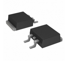
- MOSFET P-CH 60V 5.1A DPAK
- ECAD Model:
-
- Datasheet:
- IRFR9014TRR
Vishay Siliconix IRFR9014TRR technical specifications, attributes, parameters and parts with similar specifications to Vishay Siliconix IRFR9014TRR.
- MountSurface Mount
- Mounting TypeSurface Mount
- Package / CaseTO-252-3, DPak (2 Leads Tab), SC-63
- Supplier Device PackageD-Pak
- Operating Temperature-55°C~150°C TJ
- PackagingTape & Reel (TR)
- Published2016
- Part StatusActive
- Moisture Sensitivity Level (MSL)1 (Unlimited)
- TechnologyMOSFET (Metal Oxide)
- Power Dissipation-Max2.5W Ta 25W Tc
- FET TypeP-Channel
- Rds On (Max) @ Id, Vgs500mOhm @ 3.1A, 10V
- Vgs(th) (Max) @ Id4V @ 250μA
- Input Capacitance (Ciss) (Max) @ Vds270pF @ 25V
- Current - Continuous Drain (Id) @ 25°C5.1A Tc
- Gate Charge (Qg) (Max) @ Vgs12nC @ 10V
- Drain to Source Voltage (Vdss)60V
- Drive Voltage (Max Rds On,Min Rds On)10V
- Vgs (Max)±20V
- Continuous Drain Current (ID)5.1A
- Input Capacitance270pF
- Rds On Max500 mΩ
- RoHS StatusNon-RoHS Compliant
IRFR9014TRR Overview
An op amp's input capacitance is defined as the capacitance between both of its input terminals with either input grounded, and 270pF @ 25V is its maximum input capacitance.The drain current is the maximum continuous current the device can conduct, and this device has 5.1A continuous drain current (ID).For this transistor to work, a voltage 60V is required between drain and source (Vdss).Using drive voltage (10V), this device contributes to a reduction in overall power consumption.
IRFR9014TRR Features
a continuous drain current (ID) of 5.1A
a 60V drain to source voltage (Vdss)
IRFR9014TRR Applications
There are a lot of Vishay Siliconix
IRFR9014TRR applications of single MOSFETs transistors.
AC-DC Power Supply
Synchronous Rectification for ATX 1 Server I Telecom PSU
Motor drives and Uninterruptible Power Supplies
Micro Solar Inverter
DC/DC converters
Power Tools
Motor Drives and Uninterruptible Power Supples
Synchronous Rectification
Battery Protection Circuit
Telecom 1 Sever Power Supplies
IRFR9014TRR More Descriptions
Tape & Reel (TR) Surface Mount P-Channel MOSFET (Metal Oxide) Mosfet Transistor 5.1A Tc 5.1A 2.5W Ta 25W Tc 60V
MOSFET P-CH 60V 5.1A DPAK
MOSFET P-CH 60V 5.1A DPAK
The three parts on the right have similar specifications to IRFR9014TRR.
-
ImagePart NumberManufacturerMountMounting TypePackage / CaseSupplier Device PackageOperating TemperaturePackagingPublishedPart StatusMoisture Sensitivity Level (MSL)TechnologyPower Dissipation-MaxFET TypeRds On (Max) @ Id, VgsVgs(th) (Max) @ IdInput Capacitance (Ciss) (Max) @ VdsCurrent - Continuous Drain (Id) @ 25°CGate Charge (Qg) (Max) @ VgsDrain to Source Voltage (Vdss)Drive Voltage (Max Rds On,Min Rds On)Vgs (Max)Continuous Drain Current (ID)Input CapacitanceRds On MaxRoHS StatusSurface MountTransistor Element MaterialSeriesJESD-609 CodeNumber of TerminationsECCN CodeTerminal FinishAdditional FeatureSubcategoryTerminal PositionTerminal FormPeak Reflow Temperature (Cel)Reach Compliance CodeTime@Peak Reflow Temperature-Max (s)JESD-30 CodeQualification StatusOperating Temperature (Max)Number of ElementsConfigurationOperating ModeCase ConnectionTransistor ApplicationJEDEC-95 CodeDrain Current-Max (Abs) (ID)Drain-source On Resistance-MaxPulsed Drain Current-Max (IDM)DS Breakdown Voltage-MinAvalanche Energy Rating (Eas)View Compare
-
 IRFR9014TRRSurface MountSurface MountTO-252-3, DPak (2 Leads Tab), SC-63D-Pak-55°C~150°C TJTape & Reel (TR)2016Active1 (Unlimited)MOSFET (Metal Oxide)2.5W Ta 25W TcP-Channel500mOhm @ 3.1A, 10V4V @ 250μA270pF @ 25V5.1A Tc12nC @ 10V60V10V±20V5.1A270pF500 mΩNon-RoHS Compliant-----------------------------
 -
-Surface MountTO-252-3, DPak (2 Leads Tab), SC-63--Tape & Reel (TR)2004Discontinued1 (Unlimited)MOSFET (Metal Oxide)45W TcN-Channel75m Ω @ 10A, 10V4V @ 250μA370pF @ 25V17A Tc20nC @ 10V55V10V±20V---ROHS3 CompliantYESSILICONHEXFET®e32EAR99Matte Tin (Sn) - with Nickel (Ni) barrierAVALANCHE RATED, ULTRA LOW RESISTANCEFET General Purpose PowerSINGLEGULL WINGNOT SPECIFIEDnot_compliantNOT SPECIFIEDR-PSSO-G2Not Qualified175°C1SINGLE WITH BUILT-IN DIODEENHANCEMENT MODEDRAINSWITCHINGTO-252AA17A0.075Ohm68A55V71 mJ
-
-Surface MountTO-252-3, DPak (2 Leads Tab), SC-63--55°C~175°C TJTape & Reel (TR)2004Obsolete1 (Unlimited)MOSFET (Metal Oxide)48W TcN-Channel210m Ω @ 5.6A, 10V4V @ 250μA330pF @ 25V9.4A Ta25nC @ 10V100V10V±20V------HEXFET®-------------------------
-
Surface MountSurface MountTO-252-3, DPak (2 Leads Tab), SC-63--55°C~150°C TJTape & Reel (TR)2016Active1 (Unlimited)MOSFET (Metal Oxide)25W TcN-Channel200m Ω @ 4.6A, 10V4V @ 250μA250pF @ 25V8.2A Tc10nC @ 10V50V10V±20V8.2A--Non-RoHS Compliant----------------------------

Popular Search Part Number
Related Keywords
Search Tags
Latest News
-
23 April 2024
LNK304PN Manufacturer, Highlights, Functions and Other Details
Ⅰ. LNK304PN overviewⅡ. Manufacturer of LNK304PNⅢ. Highlights of LNK304PNⅣ. Pin functional description of LNK304PNⅤ. Functions of LNK304PNⅥ. How to judge the quality of LNK304PNⅦ. How to implement the... -
23 April 2024
LM331 Frequency to Voltage Converter Functions, Working Principle and Application Circuit
Ⅰ. LM331 descriptionⅡ. Functions and roles of LM331Ⅲ. LM331 internal block diagramⅣ. Working principle of LM331Ⅴ. Application circuit of LM331Ⅵ. Specific applications of LM331Ⅶ. Precautions for using LM331The... -
24 April 2024
MBRS340T3G Schottky Diode: Specifications, Highlights, Structure and Features
Ⅰ. Overview of MBRS340T3GⅡ. Geometric structure of MBRS340T3GⅢ. Specifications of MBRS340T3GⅣ. Highlights of MBRS340T3GⅤ. MBRS340T3G typical electrical characteristicsⅥ. Features of MBRS340T3GⅦ. How to use and install MBRS340T3G correctly?Ⅰ.... -
24 April 2024
MC34063 Regulator Pinout, Working Principle and Advantages
Ⅰ. What is MC34063?Ⅱ. Pin diagram and functions of MC34063Ⅲ. How does MC34063 work?Ⅳ. MC34063 boost circuit calculation methodⅤ. MC34063 step-down switching circuitⅥ. Voltage reverse circuit composed of...
Help you to save your cost and time.
Reliable package for your goods.
Fast Reliable Delivery to save time.
Quality premium after-sale service.