Texas Instruments CSD17484F4
- Part Number:
- CSD17484F4
- Manufacturer:
- Texas Instruments
- Ventron No:
- 2850212-CSD17484F4
- Description:
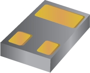
- 30-V, N channel NexFET? power MOSFET, single LGA 1 mm x 0.6mm, 128 mOhm, gate ESD protection
- ECAD Model:
-
- Datasheet:
- csd17484f4
- Lifecycle StatusACTIVE (Last Updated: 1 day ago)
- Factory Lead Time6 Weeks
- MountSurface Mount
- Mounting TypeSurface Mount
- Package / Case3-XFDFN
- Number of Pins3
- Transistor Element MaterialSILICON
- Operating Temperature-55°C~150°C TJ
- PackagingTape & Reel (TR)
- SeriesFemtoFET™
- Pbfree Codeyes
- Part StatusActive
- Moisture Sensitivity Level (MSL)1 (Unlimited)
- Number of Terminations3
- ECCN CodeEAR99
- TechnologyMOSFET (Metal Oxide)
- Terminal PositionBOTTOM
- Terminal FormNO LEAD
- Base Part NumberCSD17484
- Pin Count3
- Number of Elements1
- Power Dissipation-Max500mW Ta
- Element ConfigurationSingle
- Operating ModeENHANCEMENT MODE
- Turn On Delay Time3 ns
- FET TypeN-Channel
- Transistor ApplicationSWITCHING
- Rds On (Max) @ Id, Vgs121m Ω @ 500mA, 8V
- Vgs(th) (Max) @ Id1.1V @ 250μA
- Input Capacitance (Ciss) (Max) @ Vds195pF @ 15V
- Current - Continuous Drain (Id) @ 25°C3A Ta
- Gate Charge (Qg) (Max) @ Vgs1.2nC @ 4.5V
- Rise Time1ns
- Drain to Source Voltage (Vdss)30V
- Drive Voltage (Max Rds On,Min Rds On)1.8V 8V
- Fall Time (Typ)4 ns
- Turn-Off Delay Time11 ns
- Continuous Drain Current (ID)3A
- Gate to Source Voltage (Vgs)12V
- Drain Current-Max (Abs) (ID)3A
- Drain-source On Resistance-Max0.27Ohm
- Feedback Cap-Max (Crss)2.9 pF
- Length1.035mm
- Width635μm
- Thickness200μm
- RoHS StatusROHS3 Compliant
- Lead FreeLead Free
CSD17484F4 is a type of N-Channel FemtoFET? MOSFET optimized for load switch applications and general-purpose switching applications. It is specifically designed and optimized to minimize the footprint in many handheld and mobile applications. Based on the unique technology, CSD17484F4 is able to replace standard small signal MOSFETs while providing at least a 60% reduction in footprint size.
CSD17484F4 Features
Low on-resistance
Ultralow Qg and Qgd
Low-threshold voltage
Advanced switching performance
Available in the Femto package
CSD17484F4 Applications
Battery applications
Load switch applications
Handheld and mobile applications
General-purpose switching applications
MOSFET N-CH 30V 3A 3-PICOSTAR / 30 V N-Channel FemtoFET MOSFET
CoC and 2-years warranty / RFQ for pricing
-
ImagePart NumberManufacturerLifecycle StatusFactory Lead TimeMountMounting TypePackage / CaseNumber of PinsTransistor Element MaterialOperating TemperaturePackagingSeriesPbfree CodePart StatusMoisture Sensitivity Level (MSL)Number of TerminationsECCN CodeTechnologyTerminal PositionTerminal FormBase Part NumberPin CountNumber of ElementsPower Dissipation-MaxElement ConfigurationOperating ModeTurn On Delay TimeFET TypeTransistor ApplicationRds On (Max) @ Id, VgsVgs(th) (Max) @ IdInput Capacitance (Ciss) (Max) @ VdsCurrent - Continuous Drain (Id) @ 25°CGate Charge (Qg) (Max) @ VgsRise TimeDrain to Source Voltage (Vdss)Drive Voltage (Max Rds On,Min Rds On)Fall Time (Typ)Turn-Off Delay TimeContinuous Drain Current (ID)Gate to Source Voltage (Vgs)Drain Current-Max (Abs) (ID)Drain-source On Resistance-MaxFeedback Cap-Max (Crss)LengthWidthThicknessRoHS StatusLead FreeSurface MountVgs (Max)DS Breakdown Voltage-MinNumber of ChannelsPower DissipationCase ConnectionMax Junction Temperature (Tj)HeightView Compare
-
 CSD17484F4ACTIVE (Last Updated: 1 day ago)6 WeeksSurface MountSurface Mount3-XFDFN3SILICON-55°C~150°C TJTape & Reel (TR)FemtoFET™yesActive1 (Unlimited)3EAR99MOSFET (Metal Oxide)BOTTOMNO LEADCSD1748431500mW TaSingleENHANCEMENT MODE3 nsN-ChannelSWITCHING121m Ω @ 500mA, 8V1.1V @ 250μA195pF @ 15V3A Ta1.2nC @ 4.5V1ns30V1.8V 8V4 ns11 ns3A12V3A0.27Ohm2.9 pF1.035mm635μm200μmROHS3 CompliantLead Free---------
 -
ACTIVE (Last Updated: 2 days ago)8 Weeks-Surface Mount3-SMD, No Lead3SILICON-55°C~150°C TJTape & Reel (TR)FemtoFET™yesActive1 (Unlimited)3-MOSFET (Metal Oxide)BOTTOM-CSD13385-1500mW TaSingleENHANCEMENT MODE-N-ChannelSWITCHING19m Ω @ 900mA, 4.5V1.2V @ 250μA674pF @ 6V4.3A Ta5nC @ 4.5V-12V1.8V 4.5V-------1.49mm730μm338μmROHS3 Compliant-YES8V12V-----
-
ACTIVE (Last Updated: 1 day ago)6 WeeksSurface MountSurface Mount3-XFDFN3SILICON-55°C~150°C TJTape & Reel (TR)FemtoFET™yesActive1 (Unlimited)3EAR99MOSFET (Metal Oxide)BOTTOMNO LEADCSD17382-1500mW TaSingleENHANCEMENT MODE59 nsN-ChannelSWITCHING64m Ω @ 500mA, 8V1.2V @ 250μA347pF @ 15V2.3A Ta2.7nC @ 4.5V-30V1.8V 8V-279 ns2.3A10V---1.035mm635μm-ROHS3 CompliantLead Free---1500mWDRAIN150°C350μm
-
ACTIVE (Last Updated: 2 days ago)6 Weeks-Surface Mount3-SMD, No Lead3SILICON-55°C~150°C TJTape & Reel (TR)FemtoFET™yesActive1 (Unlimited)3EAR99MOSFET (Metal Oxide)BOTTOM-CSD13380-1500mW TaSingleENHANCEMENT MODE-N-ChannelSWITCHING76m Ω @ 400mA, 4.5V1.3V @ 250μA156pF @ 6V3.6A Ta1.2nC @ 4.5V-12V1.8V 4.5V----2.1A0.092Ohm12.5 pF690μm600μm345μmROHS3 Compliant-YES8V12V-----

-
40-V, N channel NexFET? power MOSFET, single SON 5 mm x 6 mm, 0.96 mOhm
-
12-V, N channel NexFET? power MOSFET, single LGA 0.8 mm x 1.5 mm, 19 mOhm, gate ESD protection
-
30-V, N channel NexFET? power MOSFET, single SON 5 mm x 6 mm, 2.9 mOhm
-
25-V, N channel NexFET? power MOSFET, single SON 5 mm x 6 mm, 0.82 mOhm
-
40-V, N channel NexFET? power MOSFET, single SON 5 mm x 6 mm, 1.6 mOhm
-
30-V, N channel NexFET? power MOSFET, single LGA 1 mm x 0.6mm, 128 mOhm, gate ESD protection
-
30-V, N channel NexFET? power MOSFET, single LGA 1 mm x 0.6mm, 67 mOhm, gate ESD protection
-
12-V, N channel NexFET? power MOSFET, single LGA 0.6 mm x 0.7 mm, 76 mOhm, gate ESD protection
Latest News
-
22 September 2023
LM301AN Operational Amplifier: Equivalent, Circuit and Package
Ⅰ. What is LM301AN?Ⅱ. Symbol, footprint and pin connection of LM301ANⅢ. Technical parametersⅣ. LM301AN tone control circuitⅤ. Features of LM301ANⅥ. What is the difference between LM301AN and LM709?Ⅶ.... -
25 September 2023
Get to Know the IRFB7545PBF Power MOSFET
Ⅰ. What is IRFB7545PBF?Ⅱ. Symbol and Footprint of IRFB7545PBFⅢ. Technical parametersⅣ. Features of IRFB7545PBFⅤ. Pinout and package of IRFB7545PBFⅥ. Application of IRFB7545PBFⅦ. How to use IRFB7545PBF?Ⅷ. How to... -
25 September 2023
A Comparison of 2N7000 and BS170 N-Channel Mosfet Transistors
Ⅰ. What is a MOS field effect transistor?Ⅱ. Overview of 2N7000Ⅲ. Overview of BS170Ⅳ. 2N7000 vs BS170: PCB footprintsⅤ. 2N7000 vs BS170: Technical parametersⅥ. 2N7000 vs BS170: FeaturesⅦ.... -
26 September 2023
W25Q128JVSIQ Footprint, Features and Package
Ⅰ. W25Q128JVSIQ descriptionⅡ. W25Q128JVSIQ symbol and footprintⅢ. Technical parametersⅣ. Features of W25Q128JVSIQⅤ. Pin configuration of W25Q128JVSIQⅥ. Package of W25Q128JVSIQⅦ. What are the characteristics of the SPI interface of...
Help you to save your cost and time.
Reliable package for your goods.
Fast Reliable Delivery to save time.
Quality premium after-sale service.