Texas Instruments CSD17382F4
- Part Number:
- CSD17382F4
- Manufacturer:
- Texas Instruments
- Ventron No:
- 2850135-CSD17382F4
- Description:
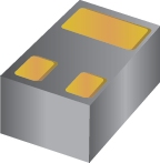
- 30-V, N channel NexFET? power MOSFET, single LGA 1 mm x 0.6mm, 67 mOhm, gate ESD protection
- ECAD Model:
-
- Datasheet:
- csd17382f4
- Lifecycle StatusACTIVE (Last Updated: 1 day ago)
- Factory Lead Time6 Weeks
- MountSurface Mount
- Mounting TypeSurface Mount
- Package / Case3-XFDFN
- Number of Pins3
- Transistor Element MaterialSILICON
- Operating Temperature-55°C~150°C TJ
- PackagingTape & Reel (TR)
- SeriesFemtoFET™
- Pbfree Codeyes
- Part StatusActive
- Moisture Sensitivity Level (MSL)1 (Unlimited)
- Number of Terminations3
- ECCN CodeEAR99
- TechnologyMOSFET (Metal Oxide)
- Terminal PositionBOTTOM
- Terminal FormNO LEAD
- Base Part NumberCSD17382
- Number of Elements1
- Number of Channels1
- Power Dissipation-Max500mW Ta
- Element ConfigurationSingle
- Operating ModeENHANCEMENT MODE
- Power Dissipation500mW
- Case ConnectionDRAIN
- Turn On Delay Time59 ns
- FET TypeN-Channel
- Transistor ApplicationSWITCHING
- Rds On (Max) @ Id, Vgs64m Ω @ 500mA, 8V
- Vgs(th) (Max) @ Id1.2V @ 250μA
- Input Capacitance (Ciss) (Max) @ Vds347pF @ 15V
- Current - Continuous Drain (Id) @ 25°C2.3A Ta
- Gate Charge (Qg) (Max) @ Vgs2.7nC @ 4.5V
- Drain to Source Voltage (Vdss)30V
- Drive Voltage (Max Rds On,Min Rds On)1.8V 8V
- Turn-Off Delay Time279 ns
- Continuous Drain Current (ID)2.3A
- Gate to Source Voltage (Vgs)10V
- Max Junction Temperature (Tj)150°C
- Height350μm
- Length1.035mm
- Width635μm
- RoHS StatusROHS3 Compliant
- Lead FreeLead Free
CSD17382F4 is a type of N-Channel FemtoFET? MOSFET optimized for load switch applications and general-purpose switching applications. It is specifically designed and optimized to minimize the footprint in many handheld and mobile applications. Based on the unique technology, CSD17382F4 is able to replace standard small signal MOSFETs while providing at least a 60% reduction in footprint size.
CSD17382F4 Features
Low on-resistance
Ultralow Qg and Qgd
Low-threshold voltage
Advanced switching performance
Available in the Femto package
CSD17382F4 Applications
Battery applications
Load switch applications
Handheld and mobile applications
General-purpose switching applications
N-Channel FemtoFET MOSFET 30V 2.3A 3-Pin PICOSTAR T/R
IC EEPROM 256K SPI 20MHZ 8SO
-
ImagePart NumberManufacturerLifecycle StatusFactory Lead TimeMountMounting TypePackage / CaseNumber of PinsTransistor Element MaterialOperating TemperaturePackagingSeriesPbfree CodePart StatusMoisture Sensitivity Level (MSL)Number of TerminationsECCN CodeTechnologyTerminal PositionTerminal FormBase Part NumberNumber of ElementsNumber of ChannelsPower Dissipation-MaxElement ConfigurationOperating ModePower DissipationCase ConnectionTurn On Delay TimeFET TypeTransistor ApplicationRds On (Max) @ Id, VgsVgs(th) (Max) @ IdInput Capacitance (Ciss) (Max) @ VdsCurrent - Continuous Drain (Id) @ 25°CGate Charge (Qg) (Max) @ VgsDrain to Source Voltage (Vdss)Drive Voltage (Max Rds On,Min Rds On)Turn-Off Delay TimeContinuous Drain Current (ID)Gate to Source Voltage (Vgs)Max Junction Temperature (Tj)HeightLengthWidthRoHS StatusLead FreeContact PlatingJESD-609 CodeTerminal FinishAdditional FeaturePeak Reflow Temperature (Cel)Reach Compliance CodeTime@Peak Reflow Temperature-Max (s)Rise TimeVgs (Max)Fall Time (Typ)Drain Current-Max (Abs) (ID)Pulsed Drain Current-Max (IDM)DS Breakdown Voltage-MinFeedback Cap-Max (Crss)ThicknessSurface MountDrain-source On Resistance-MaxAvalanche Energy Rating (Eas)Pin CountView Compare
-
 CSD17382F4ACTIVE (Last Updated: 1 day ago)6 WeeksSurface MountSurface Mount3-XFDFN3SILICON-55°C~150°C TJTape & Reel (TR)FemtoFET™yesActive1 (Unlimited)3EAR99MOSFET (Metal Oxide)BOTTOMNO LEADCSD1738211500mW TaSingleENHANCEMENT MODE500mWDRAIN59 nsN-ChannelSWITCHING64m Ω @ 500mA, 8V1.2V @ 250μA347pF @ 15V2.3A Ta2.7nC @ 4.5V30V1.8V 8V279 ns2.3A10V150°C350μm1.035mm635μmROHS3 CompliantLead Free--------------------
 -
ACTIVE (Last Updated: 1 day ago)12 WeeksSurface MountSurface Mount8-PowerTDFN8SILICON-55°C~150°C TJTape & Reel (TR)NexFET™yesActive1 (Unlimited)5EAR99MOSFET (Metal Oxide)DUALNO LEADCSD165701-3.2W Ta 195W TcSingleENHANCEMENT MODE-DRAIN5 nsN-Channel-0.59m Ω @ 50A, 10V1.9V @ 250μA14000pF @ 12V100A Ta250nC @ 10V25V4.5V 10V156 ns100A20V--5mm6mmROHS3 CompliantContains LeadGolde3Matte Tin (Sn)AVALANCHE RATED260not_compliantNOT SPECIFIED43ns±20V72 ns59A400A25V1290 pF950μm----
-
ACTIVE (Last Updated: 1 week ago)6 Weeks-Surface Mount8-PowerTDFN8SILICON-55°C~150°C TJTape & Reel (TR)NexFET™yesActive1 (Unlimited)5EAR99MOSFET (Metal Oxide)DUALNO LEADCSD185121-139W TcSingleENHANCEMENT MODE-DRAIN-N-ChannelSWITCHING1.6m Ω @ 30A, 10V2.2V @ 250μA7120pF @ 20V211A Tc-40V4.5V 10V-----5mm6mmROHS3 Compliant--e4Nickel/Palladium/Gold (Ni/Pd/Au)AVALANCHE RATED-not_compliant--±20V-32A400A40V333 pF950μmYES0.0023Ohm205 mJ-
-
ACTIVE (Last Updated: 1 day ago)6 WeeksSurface MountSurface Mount3-XFDFN3SILICON-55°C~150°C TJTape & Reel (TR)FemtoFET™yesActive1 (Unlimited)3EAR99MOSFET (Metal Oxide)BOTTOMNO LEADCSD174841-500mW TaSingleENHANCEMENT MODE--3 nsN-ChannelSWITCHING121m Ω @ 500mA, 8V1.1V @ 250μA195pF @ 15V3A Ta1.2nC @ 4.5V30V1.8V 8V11 ns3A12V--1.035mm635μmROHS3 CompliantLead Free-------1ns-4 ns3A--2.9 pF200μm-0.27Ohm-3

-
40-V, N channel NexFET? power MOSFET, single SON 5 mm x 6 mm, 0.96 mOhm
-
12-V, N channel NexFET? power MOSFET, single LGA 0.8 mm x 1.5 mm, 19 mOhm, gate ESD protection
-
30-V, N channel NexFET? power MOSFET, single SON 5 mm x 6 mm, 2.9 mOhm
-
25-V, N channel NexFET? power MOSFET, single SON 5 mm x 6 mm, 0.82 mOhm
-
40-V, N channel NexFET? power MOSFET, single SON 5 mm x 6 mm, 1.6 mOhm
-
30-V, N channel NexFET? power MOSFET, single LGA 1 mm x 0.6mm, 128 mOhm, gate ESD protection
-
30-V, N channel NexFET? power MOSFET, single LGA 1 mm x 0.6mm, 67 mOhm, gate ESD protection
-
12-V, N channel NexFET? power MOSFET, single LGA 0.6 mm x 0.7 mm, 76 mOhm, gate ESD protection
Latest News
-
27 September 2023
BC640 PNP Transistor: Features, Package and Other Details
Ⅰ. Overview of BC640Ⅱ. Symbol and footprint of BC640Ⅲ. Technical parametersⅣ. Features of BC640Ⅴ. Pinout and package of BC640Ⅵ. Application of BC640Ⅶ. How to optimize the performance of... -
27 September 2023
Introduction to the BTS7960B Motor Drive Module
Ⅰ. What is BTS7960B?Ⅱ. BTS7960B symbol, footprint and pin configurationⅢ. Technical parametersⅣ. Features of BTS7960BⅤ. What are the advantages and disadvantages of BTS7960B?Ⅵ. How to optimize the BTS7960B... -
28 September 2023
MPSA56 PNP General Purpose Transistor: Features, Working Principle and Application
Ⅰ. Overview of MPSA56Ⅱ. Symbol and footprint of MPSA56Ⅲ. Technical parametersⅣ. Features of MPSA56Ⅴ. Pinout and package of MPSA56Ⅵ. How does MPSA56 work?Ⅶ. How does the MPSA56 transistor... -
28 September 2023
TIP35C Footprint, Package, Application and Other Details
Ⅰ. Overview of TIP35CⅡ. Symbol and footprint of TIP35CⅢ. Technical parametersⅣ. Features of TIP35CⅤ. Pinout and package of TIP35CⅥ. Working principle of TIP35C audio power amplifierⅦ. Application of...
Help you to save your cost and time.
Reliable package for your goods.
Fast Reliable Delivery to save time.
Quality premium after-sale service.