Vishay Siliconix SUD40N02-08-E3
- Part Number:
- SUD40N02-08-E3
- Manufacturer:
- Vishay Siliconix
- Ventron No:
- 2852892-SUD40N02-08-E3
- Description:
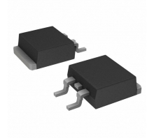
- MOSFET N-CH 20V 40A TO252
- ECAD Model:
-
- Datasheet:
- SUD40N02-08-E3
Vishay Siliconix SUD40N02-08-E3 technical specifications, attributes, parameters and parts with similar specifications to Vishay Siliconix SUD40N02-08-E3.
- MountSurface Mount
- Mounting TypeSurface Mount
- Package / CaseTO-252-3, DPak (2 Leads Tab), SC-63
- Number of Pins3
- Transistor Element MaterialSILICON
- Operating Temperature-55°C~175°C TJ
- PackagingTape & Reel (TR)
- SeriesTrenchFET®
- Published2008
- JESD-609 Codee3
- Pbfree Codeyes
- Part StatusObsolete
- Moisture Sensitivity Level (MSL)1 (Unlimited)
- Number of Terminations2
- ECCN CodeEAR99
- Terminal FinishMatte Tin (Sn) - with Nickel (Ni) barrier
- SubcategoryFET General Purpose Power
- TechnologyMOSFET (Metal Oxide)
- Terminal FormGULL WING
- Pin Count4
- JESD-30 CodeR-PSSO-G2
- Number of Elements1
- Power Dissipation-Max8.3W Ta 71W Tc
- Element ConfigurationSingle
- Operating ModeENHANCEMENT MODE
- Power Dissipation71W
- Case ConnectionDRAIN
- Turn On Delay Time20 ns
- FET TypeN-Channel
- Rds On (Max) @ Id, Vgs8.5m Ω @ 20A, 4.5V
- Vgs(th) (Max) @ Id600mV @ 250μA (Min)
- Input Capacitance (Ciss) (Max) @ Vds2660pF @ 20V
- Current - Continuous Drain (Id) @ 25°C40A Tc
- Gate Charge (Qg) (Max) @ Vgs35nC @ 4.5V
- Rise Time120ns
- Drive Voltage (Max Rds On,Min Rds On)2.5V 4.5V
- Vgs (Max)±12V
- Fall Time (Typ)20 ns
- Turn-Off Delay Time45 ns
- Continuous Drain Current (ID)40A
- Threshold Voltage600mV
- Gate to Source Voltage (Vgs)12V
- Drain-source On Resistance-Max0.0085Ohm
- Drain to Source Breakdown Voltage20V
- Dual Supply Voltage20V
- Nominal Vgs600 mV
- Height2.3876mm
- Length6.7056mm
- Width6.223mm
- REACH SVHCNo SVHC
- Radiation HardeningNo
- RoHS StatusROHS3 Compliant
SUD40N02-08-E3 Overview
Op amps with either input grounded have a fixed input capacitance parameter, CI, and this device has a 2660pF @ 20V maximal input capacitance.Devices can conduct a maximum continuous current of 3 amps in the drain area, so the continuous drain current (ID) for this device is 40A amps.In this device, the drain-source breakdown voltage is 20V and VGS=20V, so the drain-source breakdown voltage is 20V in this case.It is [45 ns] because it takes time to charge the input capacitance of the device before drain current conduction can begin.A turn-on delay time of 20 ns indicates the time it takes for the input capacitance of the device to charge before drain current conduction starts.Generally, the gate-source voltage (VGS) of a FET transistor is the voltage across its gate-source terminal, which is 12V.Normally, electrical devices are set to activate all of their operations at threshold voltages, and this transistor's threshold voltage is 600mV.A device like this reduces its overall power consumption when it uses drive voltage (2.5V 4.5V).
SUD40N02-08-E3 Features
a continuous drain current (ID) of 40A
a drain-to-source breakdown voltage of 20V voltage
the turn-off delay time is 45 ns
a threshold voltage of 600mV
SUD40N02-08-E3 Applications
There are a lot of Vishay Siliconix
SUD40N02-08-E3 applications of single MOSFETs transistors.
Synchronous Rectification for ATX 1 Server I Telecom PSU
Motor drives and Uninterruptible Power Supplies
Micro Solar Inverter
DC/DC converters
Power Tools
Motor Drives and Uninterruptible Power Supples
Synchronous Rectification
Battery Protection Circuit
Telecom 1 Sever Power Supplies
Industrial Power Supplies
SUD40N02-08-E3 More Descriptions
MOSFET; N-Channel 20V 14MOHM@2.5VGS PWM Optimized | Siliconix / Vishay SUD40N02-08-E3
Trans MOSFET N-CH 20V 40A 3-Pin(2 Tab) DPAK
N-Channel MOSFETs 20V 40A 71W
French Electronic Distributor since 1988
MOSFET, N, D-PAK; Transistor Polarity:N; Max Current Id:40A; Max Voltage Vds:20V; On State Resistance:0.0085ohm; Rds Measurement Voltage:4.5V; Max Voltage Vgs:12V; Power Dissipation:71W; Operating Temperature Range:-55°C to 175°C; Transistor Case Style:D-PAK; Alternate Case Style:D-PAK; Case Style:DPAK; Cont Current Id:40A; Max Power Dissipation Ptot:71W; Min Voltage Vgs th:0.6V; Power Dissipation Pd:71W; Pulse Current Idm:100A; Termination Type:SMD; Transistor Type:MOSFET; Typ Voltage Vds:20V; Typ Voltage Vgs th:0.6V; Voltage Vgs Rds on Measurement:4.5V
The three parts on the right have similar specifications to SUD40N02-08-E3.
-
ImagePart NumberManufacturerMountMounting TypePackage / CaseNumber of PinsTransistor Element MaterialOperating TemperaturePackagingSeriesPublishedJESD-609 CodePbfree CodePart StatusMoisture Sensitivity Level (MSL)Number of TerminationsECCN CodeTerminal FinishSubcategoryTechnologyTerminal FormPin CountJESD-30 CodeNumber of ElementsPower Dissipation-MaxElement ConfigurationOperating ModePower DissipationCase ConnectionTurn On Delay TimeFET TypeRds On (Max) @ Id, VgsVgs(th) (Max) @ IdInput Capacitance (Ciss) (Max) @ VdsCurrent - Continuous Drain (Id) @ 25°CGate Charge (Qg) (Max) @ VgsRise TimeDrive Voltage (Max Rds On,Min Rds On)Vgs (Max)Fall Time (Typ)Turn-Off Delay TimeContinuous Drain Current (ID)Threshold VoltageGate to Source Voltage (Vgs)Drain-source On Resistance-MaxDrain to Source Breakdown VoltageDual Supply VoltageNominal VgsHeightLengthWidthREACH SVHCRadiation HardeningRoHS StatusSupplier Device PackageWeightMax Operating TemperatureMin Operating TemperatureVoltage - Rated DCNumber of ChannelsDrain to Source Voltage (Vdss)Input CapacitanceDrain to Source ResistanceRds On MaxFactory Lead TimeResistancePeak Reflow Temperature (Cel)Time@Peak Reflow Temperature-Max (s)JEDEC-95 CodePulsed Drain Current-Max (IDM)Avalanche Energy Rating (Eas)Lead FreeView Compare
-
 SUD40N02-08-E3Surface MountSurface MountTO-252-3, DPak (2 Leads Tab), SC-633SILICON-55°C~175°C TJTape & Reel (TR)TrenchFET®2008e3yesObsolete1 (Unlimited)2EAR99Matte Tin (Sn) - with Nickel (Ni) barrierFET General Purpose PowerMOSFET (Metal Oxide)GULL WING4R-PSSO-G218.3W Ta 71W TcSingleENHANCEMENT MODE71WDRAIN20 nsN-Channel8.5m Ω @ 20A, 4.5V600mV @ 250μA (Min)2660pF @ 20V40A Tc35nC @ 4.5V120ns2.5V 4.5V±12V20 ns45 ns40A600mV12V0.0085Ohm20V20V600 mV2.3876mm6.7056mm6.223mmNo SVHCNoROHS3 Compliant-------------------
 -
Surface MountSurface MountTO-252-3, DPak (2 Leads Tab), SC-633--55°C~150°C TJTape & Reel (TR)TrenchFET®2007--Obsolete1 (Unlimited)----MOSFET (Metal Oxide)----4W Ta 70W TcSingle-70W-15 nsP-Channel15mOhm @ 13A, 10V1V @ 250μA (Min)3200pF @ 25V-125nC @ 10V18ns4.5V 10V±20V47 ns60 ns13A-20V----2.39mm6.73mm6.22mm--ROHS3 CompliantTO-252, (D-Pak)1.437803g150°C-55°C-30V130V3.2nF15mOhm15 mΩ--------
-
Surface MountSurface MountTO-252-3, DPak (2 Leads Tab), SC-633--55°C~175°C TJTape & Reel (TR)TrenchFET®2013--Active1 (Unlimited)----MOSFET (Metal Oxide)----3W Ta 136W Tc----8 nsN-Channel25mOhm @ 40A, 10V3V @ 250μA2400pF @ 25V40A Tc60nC @ 10V40ns10V±20V80 ns15 ns40A-20V---------ROHS3 CompliantTO-252, (D-Pak)-175°C-55°C--100V2.4nF-25 mΩ14 Weeks-------
-
Surface MountSurface MountTO-252-3, DPak (2 Leads Tab), SC-633SILICON-55°C~175°C TJTape & Reel (TR)TrenchFET®2014e3yesActive1 (Unlimited)2EAR99Matte Tin (Sn) - with Nickel (Ni) barrierFET General Purpose PowerMOSFET (Metal Oxide)GULL WING4R-PSSO-G213W Ta 136W TcSingleENHANCEMENT MODE3WDRAIN8 nsN-Channel25m Ω @ 40A, 10V3V @ 250μA2400pF @ 25V40A Tc60nC @ 10V40ns10V±20V80 ns15 ns40A3V20V-100V-3 V---No SVHCNoROHS3 Compliant-----------25mOhm26030TO-252AA70A80 mJLead Free

Popular Search Part Number
Related Keywords
Search Tags
Latest News
-
18 January 2024
What is the BTN8982TA Bridge and How Does it Work?
Ⅰ. Introduction to BTN8982TAⅡ. Block diagram of BTN8982TAⅢ. Specifications of BTN8982TAⅣ. Working principle of BTN8982TAⅤ. BTN8982TA symbol, footprint and pin configurationⅥ. Features of BTN8982TAⅦ. Application fields of BTN8982TABTN8982TA... -
18 January 2024
TPS51200DRCR: Advanced Regulator Solution for DDR Termination
Ⅰ. Overview of TPS51200DRCRⅡ. Technical parameters of TPS51200DRCRⅢ. What are the advantages of TPS51200DRCR?Ⅳ. Absolute maximum ratings of TPS51200DRCRⅤ. How to use TPS51200DRCR?Ⅵ. Where is TPS51200DRCR used?Ⅶ. TPS51200DRCR... -
19 January 2024
TXB0104PWR Alternatives, Package, Specifications and Applications
Ⅰ. TXB0104PWR overviewⅡ. Operating principle of TXB0104PWRⅢ. Package of TXB0104PWRⅣ. Specifications of TXB0104PWRⅤ. How to use TXB0104PWR?Ⅵ. What are the applications of TXB0104PWR?Ⅶ. How does TXB0104PWR realize automatic... -
19 January 2024
The Best Tutorial for ISO3082DWR
Ⅰ. Overview of ISO3082DWRⅡ. Technical parameters of ISO3082DWRⅢ. What are the characteristics of ISO3082DWR?Ⅳ. How does ISO3082DWR work?Ⅴ. ISO3082DWR symbol, footprint and pin configurationⅥ. Layout principles of ISO3082DWRⅦ....
Help you to save your cost and time.
Reliable package for your goods.
Fast Reliable Delivery to save time.
Quality premium after-sale service.