
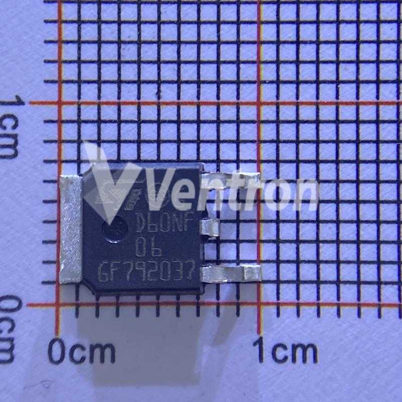
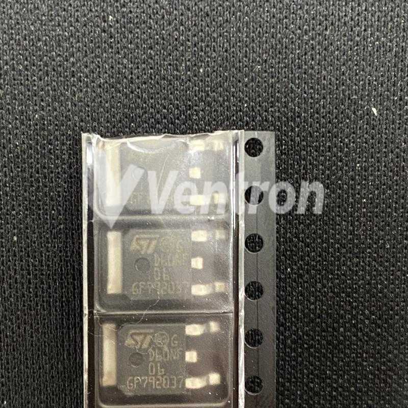
STMicroelectronics STD60NF06T4
- Part Number:
- STD60NF06T4
- Manufacturer:
- STMicroelectronics
- Ventron No:
- 2478203-STD60NF06T4
- Description:
- MOSFET N-CH 60V 60A DPAK
- ECAD Model:
-
- Datasheet:
- STD60NF06T4
STMicroelectronics STD60NF06T4 technical specifications, attributes, parameters and parts with similar specifications to STMicroelectronics STD60NF06T4.
- Lifecycle StatusACTIVE (Last Updated: 8 months ago)
- MountSurface Mount
- Mounting TypeSurface Mount
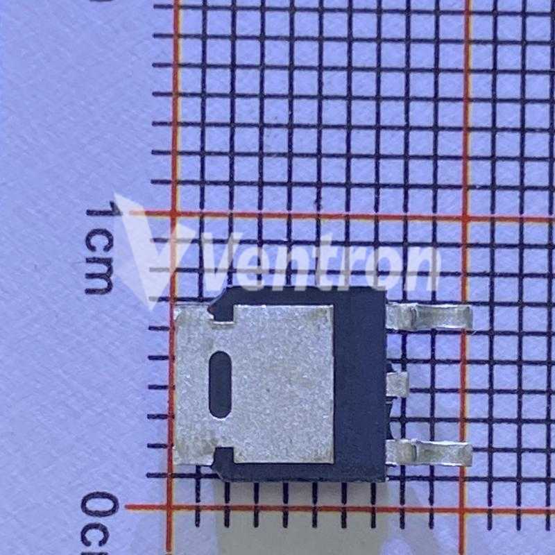
- Package / CaseTO-252-3, DPak (2 Leads Tab), SC-63
- Number of Pins3
- Transistor Element MaterialSILICON
- Operating Temperature-55°C~175°C TJ
- PackagingTape & Reel (TR)
- SeriesSTripFET™ II
- JESD-609 Codee3
- Part StatusActive
- Moisture Sensitivity Level (MSL)1 (Unlimited)
- Number of Terminations2
- ECCN CodeEAR99
- Resistance16mOhm
- Terminal FinishTin (Sn)
- SubcategoryFET General Purpose Power
- TechnologyMOSFET (Metal Oxide)
- Terminal FormGULL WING
- Peak Reflow Temperature (Cel)260
- Time@Peak Reflow Temperature-Max (s)30
- Base Part NumberSTD60N
- Pin Count3
- JESD-30 CodeR-PSSO-G2
- Number of Elements1
- Power Dissipation-Max110W Tc
- Element ConfigurationSingle
- Operating ModeENHANCEMENT MODE
- Power Dissipation110W
- Case ConnectionDRAIN
- Turn On Delay Time16 ns
- FET TypeN-Channel
- Transistor ApplicationSWITCHING
- Rds On (Max) @ Id, Vgs16m Ω @ 30A, 10V
- Vgs(th) (Max) @ Id4V @ 250μA
- Input Capacitance (Ciss) (Max) @ Vds1810pF @ 25V
- Current - Continuous Drain (Id) @ 25°C60A Tc
- Gate Charge (Qg) (Max) @ Vgs66nC @ 10V
- Rise Time108ns
- Drive Voltage (Max Rds On,Min Rds On)10V
- Vgs (Max)±20V
- Fall Time (Typ)20 ns
- Turn-Off Delay Time43 ns
- Continuous Drain Current (ID)60A
- Threshold Voltage4V
- JEDEC-95 CodeTO-252AA
- Gate to Source Voltage (Vgs)20V
- Drain to Source Breakdown Voltage60V
- Pulsed Drain Current-Max (IDM)240A
- Dual Supply Voltage60V
- Nominal Vgs4 V
- Height2.4mm
- Length6.6mm
- Width6.2mm
- REACH SVHCNo SVHC
- Radiation HardeningNo
- RoHS StatusROHS3 Compliant
- Lead FreeLead Free
STD60NF06T4 Overview
As an op amp's input capacitance parameter, CI, is defined as the capacitance between the input terminals when one input is grounded, this device's maximum input capacitance is 1810pF @ 25V.This device conducts a continuous drain current (ID) of 60A, which is the maximum continuous current transistor can conduct.Using VGS=60V and a specified value of ID, the drain-source breakdown voltage is VDS at which a specified value of ID flows. This device has a drain-source breakdown voltage of 60V (that is, no charge flow from drain to source).When the device is turned off, a turn-off delay time of 43 ns occurs as the input capacitance charges before drain current conduction commences.Pulsed drain current is maximum rated peak drain current 240A.Before drain current conduction can begin, the device's turning-on delay time takes time to charge its input capacitance. This delay time is 16 ns.Voltage at the gate-source terminal of a FET transistor, called the gate-source voltage, or VGS, can be 20V.Activation of any electrical operation happens at threshold voltage, and this transistor has 4V threshold voltage.In order to reduce power consumption, this device uses a drive voltage of 10V volts (10V).
STD60NF06T4 Features
a continuous drain current (ID) of 60A
a drain-to-source breakdown voltage of 60V voltage
the turn-off delay time is 43 ns
based on its rated peak drain current 240A.
a threshold voltage of 4V
STD60NF06T4 Applications
There are a lot of STMicroelectronics
STD60NF06T4 applications of single MOSFETs transistors.
Motor drives and Uninterruptible Power Supplies
Micro Solar Inverter
DC/DC converters
Power Tools
Motor Drives and Uninterruptible Power Supples
Synchronous Rectification
Battery Protection Circuit
Telecom 1 Sever Power Supplies
Industrial Power Supplies
PFC stages, hard switching PWM stages and resonant switching
STD60NF06T4 More Descriptions
Mosfet Transistor, N Channel, 60 A, 60 V, 14 Mohm, 10 V, 4 V |Stmicroelectronics STD60NF06T4
N-CHANNEL 60 V - 0.014 OHM - 60 A DPAK STripFET II MOSFET
MOSFET, N, D-PAK; Transistor Polarity:N Channel; Continuous Drain Current Id:60A; Source Voltage Vds:60V; On Resistance Rds(on):0.014ohm;
Power Field-Effect Transistor, 60A I(D), 60V, 0.016ohm, 1-Element, N-Channel, Silicon, Metal-oxide Semiconductor FET, TO-252AA
MOSFET, N, D-PAK; Transistor Polarity: N Channel; Continuous Drain Current Id: 60A; Drain Source Voltage Vds: 60V; On Resistance Rds(on): 0.014ohm; Rds(on) Test Voltage Vgs: 10V; Threshold Voltage Vgs: 4V; Power Dissipation Pd: 110W; Transistor Case Style: TO-252; No. of Pins: 3Pins; Operating Temperature Max: 175°C; Product Range: -; Automotive Qualification Standard: -; MSL: MSL 1 - Unlimited; SVHC: No SVHC (17-Dec-2015); Alternate Case Style: D-PAK; Current Id Max: 60A; External Depth: 10.5mm; External Length / Height: 2.55mm; External Width: 6.8mm; No. of Transistors: 1; Operating Temperature Min: -55°C; Operating Temperature Range: -55°C to 175°C; Pulse Current Idm: 240A; Voltage Vds Typ: 60V; Voltage Vgs Max: 20V; Voltage Vgs Rds on Measurement: 10V
The three parts on the right have similar specifications to STD60NF06T4.
-
ImagePart NumberManufacturerLifecycle StatusMountMounting TypePackage / CaseNumber of PinsTransistor Element MaterialOperating TemperaturePackagingSeriesJESD-609 CodePart StatusMoisture Sensitivity Level (MSL)Number of TerminationsECCN CodeResistanceTerminal FinishSubcategoryTechnologyTerminal FormPeak Reflow Temperature (Cel)Time@Peak Reflow Temperature-Max (s)Base Part NumberPin CountJESD-30 CodeNumber of ElementsPower Dissipation-MaxElement ConfigurationOperating ModePower DissipationCase ConnectionTurn On Delay TimeFET TypeTransistor ApplicationRds On (Max) @ Id, VgsVgs(th) (Max) @ IdInput Capacitance (Ciss) (Max) @ VdsCurrent - Continuous Drain (Id) @ 25°CGate Charge (Qg) (Max) @ VgsRise TimeDrive Voltage (Max Rds On,Min Rds On)Vgs (Max)Fall Time (Typ)Turn-Off Delay TimeContinuous Drain Current (ID)Threshold VoltageJEDEC-95 CodeGate to Source Voltage (Vgs)Drain to Source Breakdown VoltagePulsed Drain Current-Max (IDM)Dual Supply VoltageNominal VgsHeightLengthWidthREACH SVHCRadiation HardeningRoHS StatusLead FreeAdditional FeatureVoltage - Rated DCCurrent RatingQualification StatusDrain-source On Resistance-MaxAvalanche Energy Rating (Eas)Factory Lead TimeManufacturer Package IdentifierNumber of ChannelsMax Junction Temperature (Tj)WeightView Compare
-
 STD60NF06T4ACTIVE (Last Updated: 8 months ago)Surface MountSurface MountTO-252-3, DPak (2 Leads Tab), SC-633SILICON-55°C~175°C TJTape & Reel (TR)STripFET™ IIe3Active1 (Unlimited)2EAR9916mOhmTin (Sn)FET General Purpose PowerMOSFET (Metal Oxide)GULL WING26030STD60N3R-PSSO-G21110W TcSingleENHANCEMENT MODE110WDRAIN16 nsN-ChannelSWITCHING16m Ω @ 30A, 10V4V @ 250μA1810pF @ 25V60A Tc66nC @ 10V108ns10V±20V20 ns43 ns60A4VTO-252AA20V60V240A60V4 V2.4mm6.6mm6.2mmNo SVHCNoROHS3 CompliantLead Free------------
 -
-Through HoleThrough HoleTO-251-3 Short Leads, IPak, TO-251AA-SILICON-55°C~175°C TJTubeSTripFET™ III-Obsolete1 (Unlimited)3EAR99--FET General Purpose PowerMOSFET (Metal Oxide)-260NOT SPECIFIEDSTD60N3R-PSIP-T3170W TcSingleENHANCEMENT MODE70WDRAIN-N-ChannelSWITCHING9m Ω @ 30A, 10V1V @ 250μA2200pF @ 25V60A Tc21nC @ 5V95ns5V 10V±20V15 ns19 ns60A--20V30V240A-------ROHS3 CompliantLead FreeLOW THRESHOLD30V60ANot Qualified0.017Ohm300 mJ-----
-
ACTIVE (Last Updated: 8 months ago)Surface MountSurface MountTO-252-3, DPak (2 Leads Tab), SC-633--55°C~150°C TJCut Tape (CT)SuperMESH5™-Active1 (Unlimited)-EAR99---MOSFET (Metal Oxide)-NOT SPECIFIEDNOT SPECIFIEDSTD6N---85W Tc--85W-16 nsN-Channel-1.6 Ω @ 2A, 10V5V @ 100μA255pF @ 100V4.5A Tc7.5nC @ 10V-10V30V-28.5 ns4.5A3V-30V800V---2.52mm----ROHS3 CompliantLead Free------17 WeeksDPAK-0068772_type-E1150°C-
-
-Surface MountSurface MountTO-252-3, DPak (2 Leads Tab), SC-633--55°C~150°C TJCut Tape (CT)MDmesh™-Active1 (Unlimited)-EAR99---MOSFET (Metal Oxide)-NOT SPECIFIEDNOT SPECIFIEDSTD6N---60W Tc----19 nsN-Channel-1.35 Ω @ 2A, 10V4V @ 250μA226pF @ 100V4A Tc9.8nC @ 10V7ns10V±25V20 ns6.5 ns4A3V-25V650V------No SVHC-ROHS3 Compliant-------16 Weeks-1-3.949996g
Popular Search Part Number
Related Keywords
Search Tags
Latest News
-
23 February 2024
ADM2483BRWZ Alternatives, Symbol, Advantages and Disadvantages and Package
Ⅰ. Overview of ADM2483BRWZⅡ. Technical parameters of ADM2483BRWZⅢ. ADM2483BRWZ symbol, footprint and pin configurationⅣ. Circuit description of ADM2483BRWZⅤ. What are the advantages and disadvantages of ADM2483BRWZ?Ⅵ. Dimensions and... -
23 February 2024
LM386 Audio Amplifier IC Structure, Working Principle, Manufacturer, Function and Applications
Ⅰ. Overview of LM386Ⅱ. Internal structure and working principle of LM386Ⅲ. Pins and functions of LM386Ⅳ. Manufacturer of LM386Ⅴ. What is the function of LM386?Ⅵ. How to use... -
26 February 2024
A Complete Guide to DLW5BTM501SQ2L Common Mode Filter
Ⅰ. What is common mode filter?Ⅱ. DLW5BTM501SQ2L descriptionⅢ. Structure of DLW5BTM501SQ2L common mode filterⅣ. Who made DLW5BTM501SQ2L?Ⅴ. Frequency response range of DLW5BTM501SQ2L filterⅥ. Typical characteristics of DLW5BTM501SQ2LⅦ. Specifications... -
26 February 2024
STM32F407VGT6 Microcontroller Replacements, Application Fields and Package
Ⅰ. STM32F407VGT6 overviewⅡ. STM32F407VGT6 parameter conditionsⅢ. STM32F407VGT6 application areasⅣ. Package of STM32F407VGT6Ⅴ. Hardware design and software design of STM32F407VGT6 microcontrollerⅥ. Absolute maximum ratings of STM32F407VGT6Ⅶ. How to evaluate...
Help you to save your cost and time.
Reliable package for your goods.
Fast Reliable Delivery to save time.
Quality premium after-sale service.