Microchip Technology DN2470K4-G
- Part Number:
- DN2470K4-G
- Manufacturer:
- Microchip Technology
- Ventron No:
- 2484648-DN2470K4-G
- Description:
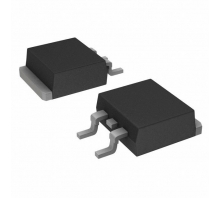
- MOSFET N-CH 700V 0.17A 3DPAK
- ECAD Model:
-
- Datasheet:
- DN2470K4-G
Microchip Technology DN2470K4-G technical specifications, attributes, parameters and parts with similar specifications to Microchip Technology DN2470K4-G.
- Factory Lead Time14 Weeks
- MountSurface Mount
- Mounting TypeSurface Mount
- Package / CaseTO-252-3, DPak (2 Leads Tab), SC-63
- Number of Pins3
- Weight3.949996g
- Transistor Element MaterialSILICON
- Operating Temperature-55°C~150°C TJ
- PackagingTape & Reel (TR)
- Published2013
- JESD-609 Codee3
- Part StatusActive
- Moisture Sensitivity Level (MSL)3 (168 Hours)
- Number of Terminations2
- ECCN CodeEAR99
- Terminal FinishMatte Tin (Sn) - annealed
- SubcategoryFET General Purpose Power
- TechnologyMOSFET (Metal Oxide)
- Terminal FormGULL WING
- Peak Reflow Temperature (Cel)NOT SPECIFIED
- Time@Peak Reflow Temperature-Max (s)NOT SPECIFIED
- Base Part NumberDN2470
- JESD-30 CodeR-PSSO-G2
- Qualification StatusNot Qualified
- Number of Elements1
- Number of Channels1
- Power Dissipation-Max2.5W Ta
- Element ConfigurationSingle
- Power Dissipation2.5W
- Case ConnectionDRAIN
- Turn On Delay Time30 ns
- FET TypeN-Channel
- Transistor ApplicationSWITCHING
- Rds On (Max) @ Id, Vgs42 Ω @ 100mA, 0V
- Input Capacitance (Ciss) (Max) @ Vds540pF @ 25V
- Current - Continuous Drain (Id) @ 25°C170mA Tj
- Rise Time45ns
- Drive Voltage (Max Rds On,Min Rds On)0V
- Vgs (Max)±20V
- Fall Time (Typ)60 ns
- Turn-Off Delay Time45 ns
- Continuous Drain Current (ID)170mA
- JEDEC-95 CodeTO-252AA
- Gate to Source Voltage (Vgs)20V
- Drain to Source Breakdown Voltage700V
- Pulsed Drain Current-Max (IDM)0.5A
- FET FeatureDepletion Mode
- Height2.5146mm
- Length6.73mm
- Width6.1mm
- RoHS StatusROHS3 Compliant
- Lead FreeLead Free
DN2470K4-G Overview
An op amp's input capacitance is defined as the capacitance between both of its input terminals with either input grounded, and 540pF @ 25V is its maximum input capacitance.The drain current is the maximum continuous current the device can conduct, and this device has 170mA continuous drain current (ID).A drainage-to-source breakdown voltage corresponds to the voltage at which a specified value of ID flows, where VGS is 700V, and this device has a drainage-to-source breakdown voltage of 700VV.Input capacitance must be charged before drain current conduction can begin, so the turn-off delay time is 45 ns.Peak drain current is 0.5A, which is the maximum pulsed drain current.Before drain current conduction begins, the device's input capacitance must be charged, so the delay time is 30 ns.An FET transistor's gate-source voltage, VGS, indicates how much voltage is applied across the transistor's gate-source terminal and it can range from 20V to 1.Using drive voltage (0V), this device contributes to a reduction in overall power consumption.
DN2470K4-G Features
a continuous drain current (ID) of 170mA
a drain-to-source breakdown voltage of 700V voltage
the turn-off delay time is 45 ns
based on its rated peak drain current 0.5A.
DN2470K4-G Applications
There are a lot of Microchip Technology
DN2470K4-G applications of single MOSFETs transistors.
AC-DC Power Supply
Synchronous Rectification for ATX 1 Server I Telecom PSU
Motor drives and Uninterruptible Power Supplies
Micro Solar Inverter
DC/DC converters
Power Tools
Motor Drives and Uninterruptible Power Supples
Synchronous Rectification
Battery Protection Circuit
Telecom 1 Sever Power Supplies
DN2470K4-G More Descriptions
Transistor MOSFET N-CH 700V 0.17A 3-Pin (2 Tab) TO-252
Power MOSFET, N Channel, 700 V, 170 mA, 42 Ohm, TO-252 (DPAK), 3 Pins, Surface Mount
MOSFET, 700V, 0.17A, 150DEG C, 2.5W; Transistor Polarity: N Channel; Continuous Drain Current Id: 170mA; Drain Source Voltage Vds: 700V; On Resistance Rds(on): 42ohm; Rds(on) Test Voltage Vgs: 0V; Threshold Voltage Vgs: -; Power Dissipation Pd: 2.5W; Transistor Case Style: TO-252; No. of Pins: 3Pins; Operating Temperature Max: 150°C; Product Range: -; Automotive Qualification Standard: -; MSL: MSL 1 - Unlimited; SVHC: No SVHC (27-Jun-2018)
Power Field-Effect Transistor, 0.17A I(D), 700V, 42ohm, 1-Element, N-Channel, Silicon, Metal-oxide Semiconductor FET, TO-252AA

Popular Search Part Number
Related Keywords
Search Tags
Latest News
-
22 September 2023
LM301AN Operational Amplifier: Equivalent, Circuit and Package
Ⅰ. What is LM301AN?Ⅱ. Symbol, footprint and pin connection of LM301ANⅢ. Technical parametersⅣ. LM301AN tone control circuitⅤ. Features of LM301ANⅥ. What is the difference between LM301AN and LM709?Ⅶ.... -
25 September 2023
Get to Know the IRFB7545PBF Power MOSFET
Ⅰ. What is IRFB7545PBF?Ⅱ. Symbol and Footprint of IRFB7545PBFⅢ. Technical parametersⅣ. Features of IRFB7545PBFⅤ. Pinout and package of IRFB7545PBFⅥ. Application of IRFB7545PBFⅦ. How to use IRFB7545PBF?Ⅷ. How to... -
25 September 2023
A Comparison of 2N7000 and BS170 N-Channel Mosfet Transistors
Ⅰ. What is a MOS field effect transistor?Ⅱ. Overview of 2N7000Ⅲ. Overview of BS170Ⅳ. 2N7000 vs BS170: PCB footprintsⅤ. 2N7000 vs BS170: Technical parametersⅥ. 2N7000 vs BS170: FeaturesⅦ.... -
26 September 2023
W25Q128JVSIQ Footprint, Features and Package
Ⅰ. W25Q128JVSIQ descriptionⅡ. W25Q128JVSIQ symbol and footprintⅢ. Technical parametersⅣ. Features of W25Q128JVSIQⅤ. Pin configuration of W25Q128JVSIQⅥ. Package of W25Q128JVSIQⅦ. What are the characteristics of the SPI interface of...

Help you to save your cost and time.
Reliable package for your goods.
Fast Reliable Delivery to save time.
Quality premium after-sale service.