
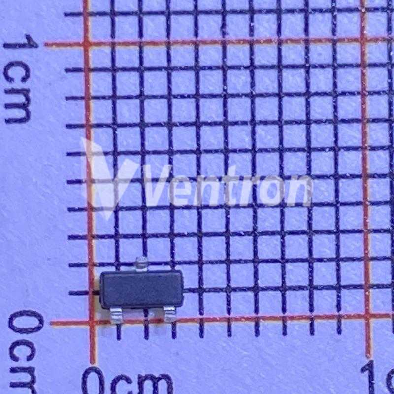
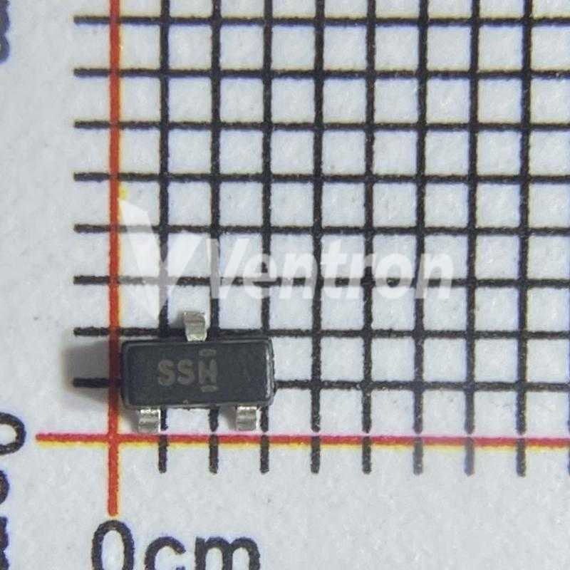
Diodes Incorporated BSS138TA
- Part Number:
- BSS138TA
- Manufacturer:
- Diodes Incorporated
- Ventron No:
- 2477992-BSS138TA
- Description:
- MOSFET N-CH 50V 200MA SOT23-3
- ECAD Model:
-
- Datasheet:
- BSS138TA

Diodes Incorporated BSS138TA technical specifications, attributes, parameters and parts with similar specifications to Diodes Incorporated BSS138TA.
- Contact PlatingTin
- MountSurface Mount
- Mounting TypeSurface Mount
- Package / CaseTO-236-3, SC-59, SOT-23-3
- Number of Pins3
- Weight7.994566mg
- Transistor Element MaterialSILICON
- Operating Temperature-55°C~150°C TJ
- PackagingCut Tape (CT)
- Published2008
- JESD-609 Codee3
- Pbfree Codeyes
- Part StatusObsolete
- Moisture Sensitivity Level (MSL)1 (Unlimited)
- Number of Terminations3
- ECCN CodeEAR99
- Resistance3.5Ohm
- SubcategoryFET General Purpose Power
- Voltage - Rated DC50V
- TechnologyMOSFET (Metal Oxide)
- Terminal PositionDUAL
- Terminal FormGULL WING
- Peak Reflow Temperature (Cel)260
- Current Rating200mA
- Time@Peak Reflow Temperature-Max (s)40
- Pin Count3
- Qualification StatusNot Qualified
- Number of Elements1
- Number of Channels1
- Power Dissipation-Max300mW Ta
- Element ConfigurationSingle
- Operating ModeENHANCEMENT MODE
- Power Dissipation360mW
- Turn On Delay Time20 ns
- FET TypeN-Channel
- Transistor ApplicationSWITCHING
- Rds On (Max) @ Id, Vgs3.5 Ω @ 220mA, 10V
- Vgs(th) (Max) @ Id1.5V @ 250μA
- Input Capacitance (Ciss) (Max) @ Vds50pF @ 10V
- Current - Continuous Drain (Id) @ 25°C200mA Ta
- Rise Time10ns
- Drive Voltage (Max Rds On,Min Rds On)10V
- Vgs (Max)±20V
- Fall Time (Typ)10 ns
- Turn-Off Delay Time20 ns
- Continuous Drain Current (ID)200mA
- Threshold Voltage1.5V
- Gate to Source Voltage (Vgs)20V
- Drain Current-Max (Abs) (ID)0.2A
- Drain to Source Breakdown Voltage50V
- Nominal Vgs1.5 V
- Feedback Cap-Max (Crss)8 pF
- Height1mm
- Length2.9mm
- Width1.3mm
- REACH SVHCNo SVHC
- RoHS StatusROHS3 Compliant
- Lead FreeLead Free
BSS138TA Overview
Op amps with either input grounded have a fixed input capacitance parameter, CI, and this device has a 50pF @ 10V maximal input capacitance.Devices can conduct a maximum continuous current of 3 amps in the drain area, so the continuous drain current (ID) for this device is 200mA amps.In this device, the drain-source breakdown voltage is 50V and VGS=50V, so the drain-source breakdown voltage is 50V in this case.A device can conduct a maximum continuous current of [0.2A] according to its drain current.It is [20 ns] because it takes time to charge the input capacitance of the device before drain current conduction can begin.A turn-on delay time of 20 ns indicates the time it takes for the input capacitance of the device to charge before drain current conduction starts.Generally, the gate-source voltage (VGS) of a FET transistor is the voltage across its gate-source terminal, which is 20V.Normally, electrical devices are set to activate all of their operations at threshold voltages, and this transistor's threshold voltage is 1.5V.A device like this reduces its overall power consumption when it uses drive voltage (10V).
BSS138TA Features
a continuous drain current (ID) of 200mA
a drain-to-source breakdown voltage of 50V voltage
the turn-off delay time is 20 ns
a threshold voltage of 1.5V
BSS138TA Applications
There are a lot of Diodes Incorporated
BSS138TA applications of single MOSFETs transistors.
Synchronous Rectification for ATX 1 Server I Telecom PSU
Motor drives and Uninterruptible Power Supplies
Micro Solar Inverter
DC/DC converters
Power Tools
Motor Drives and Uninterruptible Power Supples
Synchronous Rectification
Battery Protection Circuit
Telecom 1 Sever Power Supplies
Industrial Power Supplies
BSS138TA More Descriptions
Trans MOSFET N-CH 50V 0.2A Automotive 3-Pin SOT-23 T/R
N-Channel 50 V 3.5 Ohm Enhancement Mode FET-SOT-23 -use Diodes BSS138-7-F
Mosfet, N Channel, 50V, 200Ma, Sot-23; Transistor Polarity:n Channel; Drain Source Voltage Vds:50V; Continuous Drain Current Id:200Ma; On Resistance Rds(On):3.5Ohm; Transistor Mounting:surface Mount; Rds(On) Test Voltage Vgs:5V Rohs Compliant: Yes
MOSFET, N, 50V, SOT-23; Transistor Polarity: N Channel; Continuous Drain Current Id: 200mA; Drain Source Voltage Vds: 50V; On Resistance Rds(on): 3.5ohm; Rds(on) Test Voltage Vgs: 5V; Threshold Voltage Vgs: 1.5V; Power Dissipation Pd: 360mW; Transistor Case Style: SOT-23; No. of Pins: 3Pins; Operating Temperature Max: 150°C; Product Range: -; Automotive Qualification Standard: -; MSL: MSL 1 - Unlimited; SVHC: No SVHC (15-Jan-2019); Current Id Max: 200mA; Operating Temperature Min: -55°C; Operating Temperature Range: -55°C to 150°C; Pin Configuration: 1(G), 2(S),3(D); Pulse Current Idm: 800mA; Termination Type: Surface Mount Device; Voltage Vds Typ: 50V; Voltage Vgs Max: 20V; Voltage Vgs Rds on Measurement: 5V; Voltage Vgs th Max: 2V; Voltage Vgs th Min: 500mV
The three parts on the right have similar specifications to BSS138TA.
-
ImagePart NumberManufacturerContact PlatingMountMounting TypePackage / CaseNumber of PinsWeightTransistor Element MaterialOperating TemperaturePackagingPublishedJESD-609 CodePbfree CodePart StatusMoisture Sensitivity Level (MSL)Number of TerminationsECCN CodeResistanceSubcategoryVoltage - Rated DCTechnologyTerminal PositionTerminal FormPeak Reflow Temperature (Cel)Current RatingTime@Peak Reflow Temperature-Max (s)Pin CountQualification StatusNumber of ElementsNumber of ChannelsPower Dissipation-MaxElement ConfigurationOperating ModePower DissipationTurn On Delay TimeFET TypeTransistor ApplicationRds On (Max) @ Id, VgsVgs(th) (Max) @ IdInput Capacitance (Ciss) (Max) @ VdsCurrent - Continuous Drain (Id) @ 25°CRise TimeDrive Voltage (Max Rds On,Min Rds On)Vgs (Max)Fall Time (Typ)Turn-Off Delay TimeContinuous Drain Current (ID)Threshold VoltageGate to Source Voltage (Vgs)Drain Current-Max (Abs) (ID)Drain to Source Breakdown VoltageNominal VgsFeedback Cap-Max (Crss)HeightLengthWidthREACH SVHCRoHS StatusLead FreeSeriesGate Charge (Qg) (Max) @ VgsDrain to Source Voltage (Vdss)Surface MountTerminal FinishAdditional FeatureHTS CodeJESD-30 CodeConfigurationDrain-source On Resistance-MaxDS Breakdown Voltage-MinView Compare
-
 BSS138TATinSurface MountSurface MountTO-236-3, SC-59, SOT-23-337.994566mgSILICON-55°C~150°C TJCut Tape (CT)2008e3yesObsolete1 (Unlimited)3EAR993.5OhmFET General Purpose Power50VMOSFET (Metal Oxide)DUALGULL WING260200mA403Not Qualified11300mW TaSingleENHANCEMENT MODE360mW20 nsN-ChannelSWITCHING3.5 Ω @ 220mA, 10V1.5V @ 250μA50pF @ 10V200mA Ta10ns10V±20V10 ns20 ns200mA1.5V20V0.2A50V1.5 V8 pF1mm2.9mm1.3mmNo SVHCROHS3 CompliantLead Free------------
 -
--Surface MountTO-236-3, SC-59, SOT-23-3----55°C~150°C TJTape & Reel (TR)2012--Discontinued1 (Unlimited)-----MOSFET (Metal Oxide)---------360mW Ta----N-Channel-3.5 Ω @ 230mA, 10V1.4V @ 250μA41pF @ 25V230mA Ta-4.5V 10V±20V-------------ROHS3 Compliant-SIPMOS®1.4nC @ 10V60V--------
-
--Surface MountTO-236-3, SC-59, SOT-23-3--SILICON-55°C~150°C TJTape & Reel (TR)-e0-Obsolete1 (Unlimited)3EAR99-FET General Purpose Power-MOSFET (Metal Oxide)DUALGULL WING----Not Qualified1-360mW Ta-ENHANCEMENT MODE--N-ChannelSWITCHING6 Ω @ 170mA, 10V1.8V @ 50μA69pF @ 25V170mA Ta-4.5V 10V±20V-----0.17A--6 pF----Non-RoHS Compliant-SIPMOS®2.67nC @ 10V100VYESTin/Lead (Sn/Pb)LOGIC LEVEL COMPATIBLE8541.21.00.95R-PDSO-G3SINGLE WITH BUILT-IN DIODE10Ohm100V
-
--Surface MountTO-236-3, SC-59, SOT-23-3----55°C~150°C TJTape & Reel (TR)2002--Obsolete1 (Unlimited)-----MOSFET (Metal Oxide)---------360mW Ta----N-Channel-6 Ω @ 170mA, 10V2.3V @ 50μA78pF @ 25V170mA Ta-4.5V 10V±20V---------------SIPMOS®2.5nC @ 10V100V--------
Popular Search Part Number
Related Keywords
Search Tags
Latest News
-
19 April 2024
ADM2587EBRWZ Transceiver Pinout, Features, Application and Use
Ⅰ. Overview of ADM2587EBRWZⅡ. Pin diagram of ADM2587EBRWZⅢ. Main features of ADM2587EBRWZⅣ. Typical applications of ADM2587EBRWZⅤ. Instructions for use of ADM2587EBRWZⅥ. Power isolation and signal isolation of ADM2587EBRWZⅦ.... -
19 April 2024
Introduction to the TPS5430 DC-DC Converter
Ⅰ. TPS5430 descriptionⅡ. Pin arrangement and description of TPS5430Ⅲ. Characteristics of TPS5430Ⅳ. Functional modes of TPS5430Ⅴ. What are the advantages and disadvantages of TPS5430?Ⅵ. Application of TPS5430 in... -
22 April 2024
DRV8870DDAR H-Bridge Motor Driver: Alternatives, Functional Modes, Features and More
Ⅰ. Overview of DRV8870DDARⅡ. Device functional modesⅢ. Technical parameters of DRV8870DDARⅣ. What are the power consumption characteristics of DRV8870DDAR?Ⅴ. DRV8870DDAR circuit diagramⅥ. Power supply recommendations of DRV8870DDARⅦ. Functional... -
22 April 2024
74LS161 4-BIt Synchronous Counter Functions and Applications
Ⅰ. Introduction to 74LS161Ⅱ. Pin arrangement of 74LS161Ⅲ. Working principle of 74LS161Ⅳ. 74LS161 function tableⅤ. Basic applications of 74LS161Ⅵ. How to choose the appropriate 74LS161 counter?Ⅶ. The difference...
Help you to save your cost and time.
Reliable package for your goods.
Fast Reliable Delivery to save time.
Quality premium after-sale service.