
Fairchild/ON Semiconductor FDS3672
- Part Number:
- FDS3672
- Manufacturer:
- Fairchild/ON Semiconductor
- Ventron No:
- 2478161-FDS3672
- Description:
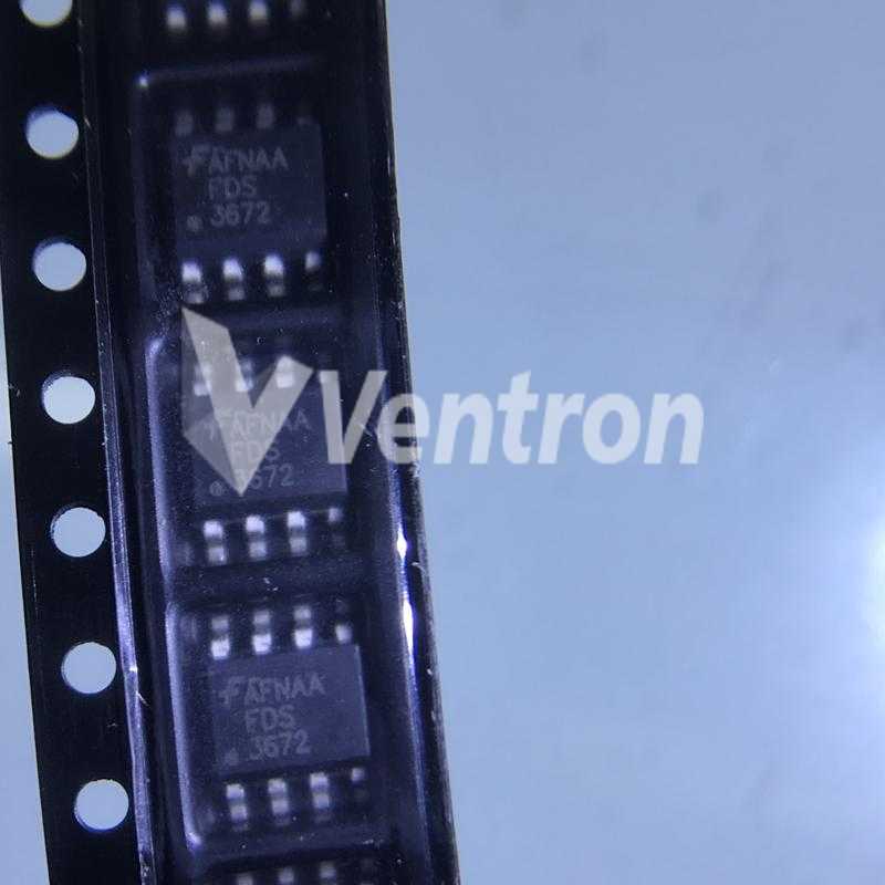
- MOSFET N-CH 100V 7.5A 8-SOIC
- ECAD Model:
-
- Datasheet:
- FDS3672
Fairchild/ON Semiconductor FDS3672 technical specifications, attributes, parameters and parts with similar specifications to Fairchild/ON Semiconductor FDS3672.
- Lifecycle StatusACTIVE (Last Updated: 1 day ago)
- Factory Lead Time12 Weeks
- MountSurface Mount
- Mounting TypeSurface Mount
- Package / Case8-SOIC (0.154, 3.90mm Width)
- Number of Pins8
- Weight130mg
- Transistor Element MaterialSILICON
- Operating Temperature-55°C~150°C TJ
- PackagingTape & Reel (TR)
- SeriesPowerTrench®
- Published2003
- JESD-609 Codee3
- Pbfree Codeyes
- Part StatusActive
- Moisture Sensitivity Level (MSL)1 (Unlimited)
- Number of Terminations8
- TerminationSMD/SMT
- ECCN CodeEAR99
- Resistance19MOhm
- Terminal FinishTin (Sn)
- SubcategoryFET General Purpose Power
- Voltage - Rated DC100V
- TechnologyMOSFET (Metal Oxide)
- Terminal PositionDUAL
- Terminal FormGULL WING
- Current Rating7.5A
- Number of Elements1
- Power Dissipation-Max2.5W Ta
- Element ConfigurationSingle
- Operating ModeENHANCEMENT MODE
- Power Dissipation2.5W
- Turn On Delay Time14 ns
- FET TypeN-Channel
- Transistor ApplicationSWITCHING
- Rds On (Max) @ Id, Vgs23m Ω @ 7.5A, 10V
- Vgs(th) (Max) @ Id4V @ 250μA
- Input Capacitance (Ciss) (Max) @ Vds2015pF @ 25V
- Current - Continuous Drain (Id) @ 25°C7.5A Ta
- Gate Charge (Qg) (Max) @ Vgs37nC @ 10V
- Rise Time20ns
- Drive Voltage (Max Rds On,Min Rds On)6V 10V
- Vgs (Max)±20V
- Fall Time (Typ)27 ns
- Turn-Off Delay Time37 ns
- Continuous Drain Current (ID)7.5A
- Threshold Voltage4V
- Gate to Source Voltage (Vgs)20V
- Drain to Source Breakdown Voltage100V
- Dual Supply Voltage100V
- Nominal Vgs4 V
- Height1.5mm
- Length5mm
- Width4mm
- REACH SVHCNo SVHC
- Radiation HardeningNo
- RoHS StatusROHS3 Compliant
- Lead FreeLead Free
FDS3672 Description
FDS3672 is an N-Channel PowerTrench? MOSFET with a voltage of 100V from the manufacturer of ON Semiconductor. The operating temperature of FDS3672 is -55°C~150°C TJ and its maximum power dissipation are 2.5W Ta. It is available in 8-SOIC (0.154, 3.90mm Width) packaging way and it has 8 pins.
FDS3672 Features
RDS(ON) = 19mΩ (Typ.), VGS = 10V, ID = 7.5A
Qg(TOT) = 28nC (Typ.), VGS = 10V
Low Miller Charge
Low QRR Body Diode
Optimized efficiency at high frequencies
UIS Capability (Single Pulse and Repetitive Pulse)
FDS3672 Applications
This product is general usage and suitable for many different applications.
DC/DC Converters
Off-line UPS
Distributed Power Architectures and VRMs
Primary Switch for 24V and 48V Systems
High Voltage Synchronous Rectifier
FDS3672 More Descriptions
MOSFET N-CH 100V 7.5A 8-SOIC / Trans MOSFET N-CH 100V 7.5A 8-Pin SOIC T/R
N-Channel PowerTrench® MOSFET, 100V, 7.5A, 22mΩ
N-Channel 100 V 22 mOhm PowerTrench Mosfet SOIC-8
Power Field-Effect Transistor, 7.5A I(D), 100V, 0.023ohm, 1-Element, N-Channel, Silicon, Metal-oxide Semiconductor FET, MS-012AA
Transistor Polarity = N-Channel / Configuration = Single / Continuous Drain Current (Id) A = 7.5 / Drain-Source Voltage (Vds) V = 100 / ON Resistance (Rds(on)) mOhm = 23 / Gate-Source Voltage V = 20 / Fall Time ns = 27 / Rise Time ns = 20 / Turn-OFF Delay Time ns = 37 / Turn-ON Delay Time ns = 14 / Operating Temperature Min. °C = -55 / Operating Temperature Max. °C = 150 / Package Type = SOIC / Pins = 8 / Mounting Type = SMD / MSL = Level-1 / Packaging = Tape & Reel / Reflow Temperature Max. °C = 260 / Power Dissipation (Pd) W = 2.5
The three parts on the right have similar specifications to FDS3672.
-
ImagePart NumberManufacturerLifecycle StatusFactory Lead TimeMountMounting TypePackage / CaseNumber of PinsWeightTransistor Element MaterialOperating TemperaturePackagingSeriesPublishedJESD-609 CodePbfree CodePart StatusMoisture Sensitivity Level (MSL)Number of TerminationsTerminationECCN CodeResistanceTerminal FinishSubcategoryVoltage - Rated DCTechnologyTerminal PositionTerminal FormCurrent RatingNumber of ElementsPower Dissipation-MaxElement ConfigurationOperating ModePower DissipationTurn On Delay TimeFET TypeTransistor ApplicationRds On (Max) @ Id, VgsVgs(th) (Max) @ IdInput Capacitance (Ciss) (Max) @ VdsCurrent - Continuous Drain (Id) @ 25°CGate Charge (Qg) (Max) @ VgsRise TimeDrive Voltage (Max Rds On,Min Rds On)Vgs (Max)Fall Time (Typ)Turn-Off Delay TimeContinuous Drain Current (ID)Threshold VoltageGate to Source Voltage (Vgs)Drain to Source Breakdown VoltageDual Supply VoltageNominal VgsHeightLengthWidthREACH SVHCRadiation HardeningRoHS StatusLead FreeContact PlatingDrain Current-Max (Abs) (ID)Surface MountPeak Reflow Temperature (Cel)Reach Compliance CodeTime@Peak Reflow Temperature-Max (s)Pin CountJESD-30 CodeQualification StatusConfigurationCase ConnectionDrain to Source Voltage (Vdss)Drain-source On Resistance-MaxPulsed Drain Current-Max (IDM)DS Breakdown Voltage-MinAvalanche Energy Rating (Eas)View Compare
-
 FDS3672ACTIVE (Last Updated: 1 day ago)12 WeeksSurface MountSurface Mount8-SOIC (0.154, 3.90mm Width)8130mgSILICON-55°C~150°C TJTape & Reel (TR)PowerTrench®2003e3yesActive1 (Unlimited)8SMD/SMTEAR9919MOhmTin (Sn)FET General Purpose Power100VMOSFET (Metal Oxide)DUALGULL WING7.5A12.5W TaSingleENHANCEMENT MODE2.5W14 nsN-ChannelSWITCHING23m Ω @ 7.5A, 10V4V @ 250μA2015pF @ 25V7.5A Ta37nC @ 10V20ns6V 10V±20V27 ns37 ns7.5A4V20V100V100V4 V1.5mm5mm4mmNo SVHCNoROHS3 CompliantLead Free-----------------
 -
ACTIVE (Last Updated: 1 day ago)9 WeeksSurface MountSurface Mount8-SOIC (0.154, 3.90mm Width)8130mgSILICON-55°C~150°C TJTape & Reel (TR)PowerTrench®-e3yesActive1 (Unlimited)8-EAR9939MOhm-FET General Purpose Power80VMOSFET (Metal Oxide)DUALGULL WING6.5A12.5W TaSingleENHANCEMENT MODE2.5W11 nsN-ChannelSWITCHING39m Ω @ 6.5A, 10V4V @ 250μA1180pF @ 40V6.5A Ta35nC @ 10V8ns6V 10V±20V12 ns26 ns6.5A4V20V80V--1.5mm5mm4mmNo SVHCNoROHS3 CompliantLead FreeTin6.4A--------------
-
---Surface Mount8-SOIC (0.154, 3.90mm Width)--SILICON-55°C~150°C TJTape & Reel (TR)PowerTrench®-e4yesObsolete1 (Unlimited)8---NICKEL PALLADIUM GOLD--MOSFET (Metal Oxide)DUALGULL WING-13W Ta-ENHANCEMENT MODE--N-ChannelSWITCHING26m Ω @ 6.7A, 10V4V @ 250μA2.714pF @ 50V6.7A Ta77nC @ 10V-6V 10V±20V-------------ROHS3 Compliant--6.7AYES260unknownNOT SPECIFIED8R-PDSO-G8COMMERCIALSINGLE WITH BUILT-IN DIODEDRAIN100V0.026Ohm60A100V360 mJ
-
ACTIVE (Last Updated: 1 day ago)9 WeeksSurface MountSurface Mount8-SOIC (0.154, 3.90mm Width)8130mgSILICON-55°C~175°C TJTape & Reel (TR)PowerTrench®-e3yesActive1 (Unlimited)8-EAR99-Tin (Sn)FET General Purpose Power80VMOSFET (Metal Oxide)DUALGULL WING4A12.5W TaSingleENHANCEMENT MODE2.5W7 nsN-ChannelSWITCHING70m Ω @ 4A, 10V4V @ 250μA634pF @ 40V4A Ta18nC @ 10V3ns6V 10V±20V4 ns24 ns4A-20V80V------NoROHS3 CompliantLead Free-4A----------0.07Ohm---
Popular Search Part Number
Related Keywords
Search Tags
Latest News
-
21 February 2024
EPCS16SI8N Manufacturer, Market Trend, Application Fields and More
Ⅰ. Overview of EPCS16SI8NⅡ. Manufacturer of EPCS16SI8NⅢ. Specifications of EPCS16SI8NⅣ. Dimensions and package of EPCS16SI8NⅤ. Functional description of EPCS16SI8NⅥ. Application fields of EPCS16SI8NⅦ. Market trend of EPCS16SI8NⅧ. How... -
21 February 2024
What is the ADS1118IDGSR and How Does it Work?
Ⅰ. ADS1118IDGSR descriptionⅡ. Specifications of ADS1118IDGSRⅢ. Absolute maximum ratings of ADS1118IDGSRⅣ. How does ADS1118IDGSR work?Ⅴ. Package of ADS1118IDGSRⅥ. What are the characteristics of ADS1118IDGSR?Ⅶ. Typical application of ADS1118IDGSRⅧ.... -
22 February 2024
L293D Motor Driver Characteristics, Technical Parameters, Advantages and Working Principle
Ⅰ. L293D descriptionⅡ. Characteristics of L293DⅢ. Technical parameters of L293DⅣ. Advantages of L293DⅤ. L293D motor driving principleⅥ. Circuit diagram of L293DⅦ. Applications of L293DⅧ. Wiring method of L293D... -
22 February 2024
L7805CV Specifications, Applications and Design Considerations
Ⅰ. Introduction to L7805CVⅡ. Specifications of L7805CVⅢ. L7805CV symbol, footprint and pin configurationⅣ. Applications of L7805CVⅤ. Precautions for using L7805CVⅥ. Absolute maximum ratings of L7805CVⅦ. Design considerations for...
Help you to save your cost and time.
Reliable package for your goods.
Fast Reliable Delivery to save time.
Quality premium after-sale service.