
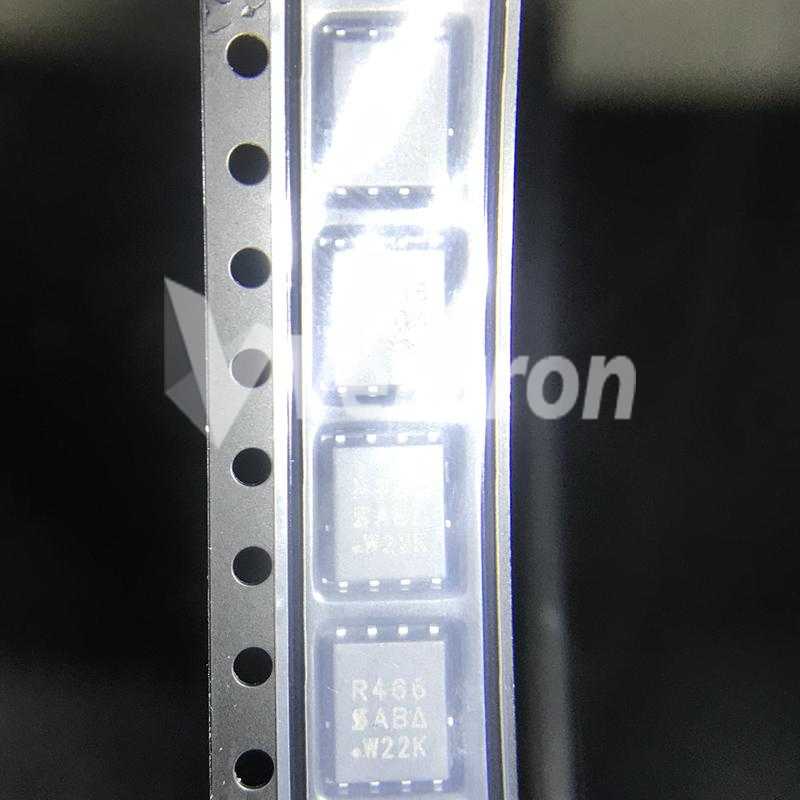
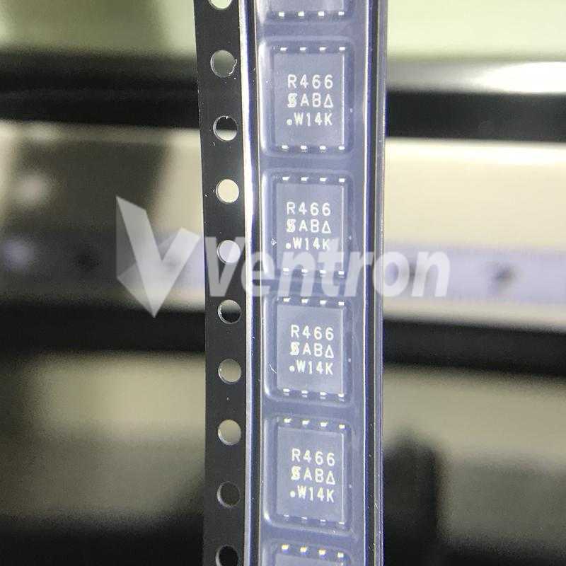
Vishay Siliconix SIR466DP-T1-GE3
- Part Number:
- SIR466DP-T1-GE3
- Manufacturer:
- Vishay Siliconix
- Ventron No:
- 2479591-SIR466DP-T1-GE3
- Description:
- MOSFET N-CH 30V 40A PPAK SO-8
- ECAD Model:
-
- Datasheet:
- SIR466DP-T1-GE3


Vishay Siliconix SIR466DP-T1-GE3 technical specifications, attributes, parameters and parts with similar specifications to Vishay Siliconix SIR466DP-T1-GE3.
- Factory Lead Time14 Weeks
- MountSurface Mount
- Mounting TypeSurface Mount
- Package / CasePowerPAK® SO-8
- Number of Pins8
- Weight506.605978mg
- Transistor Element MaterialSILICON
- Operating Temperature-55°C~150°C TJ
- PackagingTape & Reel (TR)
- SeriesTrenchFET®
- Published2013
- JESD-609 Codee3
- Pbfree Codeyes
- Part StatusActive
- Moisture Sensitivity Level (MSL)1 (Unlimited)
- Number of Terminations5
- ECCN CodeEAR99
- Resistance3.5mOhm
- Terminal FinishMATTE TIN
- SubcategoryFET General Purpose Power
- TechnologyMOSFET (Metal Oxide)
- Terminal PositionDUAL
- Terminal FormC BEND
- Peak Reflow Temperature (Cel)260
- Time@Peak Reflow Temperature-Max (s)40
- Pin Count8
- JESD-30 CodeR-XDSO-C5
- Qualification StatusNot Qualified
- Number of Elements1
- Number of Channels1
- Power Dissipation-Max5W Ta 54W Tc
- Element ConfigurationSingle
- Operating ModeENHANCEMENT MODE
- Power Dissipation5W
- Case ConnectionDRAIN
- Turn On Delay Time30 ns
- FET TypeN-Channel
- Transistor ApplicationSWITCHING
- Rds On (Max) @ Id, Vgs3.5m Ω @ 15A, 10V
- Vgs(th) (Max) @ Id2.4V @ 250μA
- Input Capacitance (Ciss) (Max) @ Vds2730pF @ 15V
- Current - Continuous Drain (Id) @ 25°C40A Tc
- Gate Charge (Qg) (Max) @ Vgs65nC @ 10V
- Rise Time9ns
- Drive Voltage (Max Rds On,Min Rds On)4.5V 10V
- Vgs (Max)±20V
- Fall Time (Typ)9 ns
- Turn-Off Delay Time35 ns
- Continuous Drain Current (ID)40A
- Threshold Voltage2.4V
- Gate to Source Voltage (Vgs)20V
- Drain to Source Breakdown Voltage30V
- Pulsed Drain Current-Max (IDM)70A
- Avalanche Energy Rating (Eas)45 mJ
- Height1.04mm
- Length4.9mm
- Width5.89mm
- REACH SVHCUnknown
- RoHS StatusROHS3 Compliant
- Lead FreeLead Free
SIR466DP-T1-GE3 Overview
The MOSFET's breakdown is called "avalanche break down", and the avalanche energy applied to transistor is rated as 45 mJ (Eas).An op amp's input capacitance is defined as the capacitance between both of its input terminals with either input grounded, and 2730pF @ 15V is its maximum input capacitance.The drain current is the maximum continuous current the device can conduct, and this device has 40A continuous drain current (ID).A drainage-to-source breakdown voltage corresponds to the voltage at which a specified value of ID flows, where VGS is 30V, and this device has a drainage-to-source breakdown voltage of 30VV.Input capacitance must be charged before drain current conduction can begin, so the turn-off delay time is 35 ns.Peak drain current is 70A, which is the maximum pulsed drain current.Before drain current conduction begins, the device's input capacitance must be charged, so the delay time is 30 ns.An FET transistor's gate-source voltage, VGS, indicates how much voltage is applied across the transistor's gate-source terminal and it can range from 20V to 1.In this case, the threshold voltage of the transistor is 2.4V, which means that it will not activate any of its functions when its threshold voltage reaches 2.4V.Using drive voltage (4.5V 10V), this device contributes to a reduction in overall power consumption.
SIR466DP-T1-GE3 Features
the avalanche energy rating (Eas) is 45 mJ
a continuous drain current (ID) of 40A
a drain-to-source breakdown voltage of 30V voltage
the turn-off delay time is 35 ns
based on its rated peak drain current 70A.
a threshold voltage of 2.4V
SIR466DP-T1-GE3 Applications
There are a lot of Vishay Siliconix
SIR466DP-T1-GE3 applications of single MOSFETs transistors.
AC-DC Power Supply
Synchronous Rectification for ATX 1 Server I Telecom PSU
Motor drives and Uninterruptible Power Supplies
Micro Solar Inverter
DC/DC converters
Power Tools
Motor Drives and Uninterruptible Power Supples
Synchronous Rectification
Battery Protection Circuit
Telecom 1 Sever Power Supplies
SIR466DP-T1-GE3 More Descriptions
Single N-Channel 30 V 3.5 mOhms Surface Mount Power Mosfet - PowerPAK SO-8
Transistor; Transistor Type:MOSFET; Continuous Drain Current, Id:40000mA; Drain Source Voltage, Vds:30V; On Resistance, Rds(on):0.0051ohm; Rds(on) Test Voltage, Vgs:20V; Threshold Voltage, Vgs Typ:2.4V; Power Dissipation, Pd:5W ;RoHS Compliant: Yes
MOSFET, N CH, 30V, 0.0029OHM, 40A, SOIC; Transistor Polarity:N Channel; Continuous Drain Current Id:40A; Drain Source Voltage Vds:30V; On Resistance Rds(on):0.0029ohm; Rds(on) Test Voltage Vgs:10V; Power Dissipation Pd:54W; Operating Temperature Min:-55°C; Operating Temperature Max:150°C; Transistor Case Style:SOIC; No. of Pins:8; MSL:-
The three parts on the right have similar specifications to SIR466DP-T1-GE3.
-
ImagePart NumberManufacturerFactory Lead TimeMountMounting TypePackage / CaseNumber of PinsWeightTransistor Element MaterialOperating TemperaturePackagingSeriesPublishedJESD-609 CodePbfree CodePart StatusMoisture Sensitivity Level (MSL)Number of TerminationsECCN CodeResistanceTerminal FinishSubcategoryTechnologyTerminal PositionTerminal FormPeak Reflow Temperature (Cel)Time@Peak Reflow Temperature-Max (s)Pin CountJESD-30 CodeQualification StatusNumber of ElementsNumber of ChannelsPower Dissipation-MaxElement ConfigurationOperating ModePower DissipationCase ConnectionTurn On Delay TimeFET TypeTransistor ApplicationRds On (Max) @ Id, VgsVgs(th) (Max) @ IdInput Capacitance (Ciss) (Max) @ VdsCurrent - Continuous Drain (Id) @ 25°CGate Charge (Qg) (Max) @ VgsRise TimeDrive Voltage (Max Rds On,Min Rds On)Vgs (Max)Fall Time (Typ)Turn-Off Delay TimeContinuous Drain Current (ID)Threshold VoltageGate to Source Voltage (Vgs)Drain to Source Breakdown VoltagePulsed Drain Current-Max (IDM)Avalanche Energy Rating (Eas)HeightLengthWidthREACH SVHCRoHS StatusLead FreeDrain to Source Voltage (Vdss)Drain-source On Resistance-MaxDS Breakdown Voltage-MinRadiation HardeningContact PlatingSurface MountConfigurationDrain Current-Max (Abs) (ID)View Compare
-
 SIR466DP-T1-GE314 WeeksSurface MountSurface MountPowerPAK® SO-88506.605978mgSILICON-55°C~150°C TJTape & Reel (TR)TrenchFET®2013e3yesActive1 (Unlimited)5EAR993.5mOhmMATTE TINFET General Purpose PowerMOSFET (Metal Oxide)DUALC BEND260408R-XDSO-C5Not Qualified115W Ta 54W TcSingleENHANCEMENT MODE5WDRAIN30 nsN-ChannelSWITCHING3.5m Ω @ 15A, 10V2.4V @ 250μA2730pF @ 15V40A Tc65nC @ 10V9ns4.5V 10V±20V9 ns35 ns40A2.4V20V30V70A45 mJ1.04mm4.9mm5.89mmUnknownROHS3 CompliantLead Free---------
 -
-Surface MountSurface MountPowerPAK® SO-8-506.605978mgSILICON-55°C~150°C TJTape & Reel (TR)TrenchFET®2016e3-Obsolete1 (Unlimited)5EAR99-MATTE TINFET General Purpose PowersMOSFET (Metal Oxide)DUALC BEND260408R-PDSO-C5-115W Ta 27.7W TcSingleENHANCEMENT MODE-DRAIN-N-ChannelSWITCHING5.6m Ω @ 20A, 10V2.3V @ 250μA1575pF @ 15V35A Tc38nC @ 10V-4.5V 10V±20V--35A-20V-70A20 mJ----ROHS3 Compliant-30V0.0075Ohm30VNo----
-
10 WeeksSurface MountSurface MountPowerPAK® SO-88506.605978mgSILICON-55°C~150°C TJTape & Reel (TR)TrenchFET®2015e3yesObsolete1 (Unlimited)5EAR9912mOhm-FET General Purpose PowerMOSFET (Metal Oxide)DUALC BEND260408R-PDSO-C5-113.9W Ta 29.8W TcSingleENHANCEMENT MODE3.9WDRAIN16 nsN-ChannelSWITCHING12m Ω @ 13.8A, 10V2.5V @ 250μA820pF @ 15V20A Tc23nC @ 10V12ns4.5V 10V±20V10 ns16 ns20A2.5V20V30V50A24 mJ1.04mm4.9mm5.89mmUnknownROHS3 CompliantLead Free---NoTin---
-
--Surface MountPowerPAK® SO-8--SILICON-55°C~150°C TJTape & Reel (TR)TrenchFET®2013-yesObsolete1 (Unlimited)5EAR99--FET General Purpose PowerMOSFET (Metal Oxide)DUALC BEND260408R-PDSO-C5Not Qualified1-5W Ta 54W Tc-ENHANCEMENT MODE-DRAIN-N-ChannelSWITCHING30.6m Ω @ 8.6A, 10V4V @ 250μA1170pF @ 50V28.4A Tc32nC @ 10V-7.5V 10V±20V------40A14.5 mJ----ROHS3 Compliant-100V0.0306Ohm100V--YESSINGLE WITH BUILT-IN DIODE8.6A
Popular Search Part Number
Related Keywords
Search Tags
Latest News
-
30 January 2024
AD7606BSTZ Converter Technical Parameters, Characteristics, Working Principle and Package
Ⅰ. Overview of AD7606BSTZⅡ. Technical parameters of AD7606BSTZⅢ. Characteristics of AD7606BSTZⅣ. Absolute maximum ratings of AD7606BSTZⅤ. How does AD7606BSTZ work?Ⅵ. Package of AD7606BSTZⅦ. What are the applications of... -
30 January 2024
LSM6DS3TR Alternatives, Features, Specifications, LSM6DS3TR vs LSM6DS3 and Applications
Ⅰ. Introduction to LSM6DS3TRⅡ. What are the features of LSM6DS3TR?Ⅲ. Absolute maximum ratings of LSM6DS3TRⅣ. Specifications of LSM6DS3TRⅤ. What are the advantages and disadvantages of LSM6DS3TR?Ⅵ. What is... -
31 January 2024
ISO1050DUBR Characteristics, Application Fields, Layout Guidelines and More
Ⅰ. What is a CAN transceiver?Ⅱ. Overview of ISO1050DUBRⅢ. Technical parameters of ISO1050DUBRⅣ. Characteristics of ISO1050DUBRⅤ. ISO1050DUBR symbol, footprint and pin configurationⅥ. Application fields of ISO1050DUBRⅦ. Layout guidelines... -
31 January 2024
TXS0108EPWR Level Shifter Specifications, Architecture, Functions, Package and Applications
Ⅰ. What is TXS0108EPWR?Ⅱ. Specifications of TXS0108EPWRⅢ. Architecture of TXS0108EPWRⅣ. Functions of TXS0108EPWRⅤ. Package of TXS0108EPWRⅥ. What are the advantages and disadvantages of TXS0108EPWR?Ⅶ. Where is TXS0108EPWR used?The...
Help you to save your cost and time.
Reliable package for your goods.
Fast Reliable Delivery to save time.
Quality premium after-sale service.