
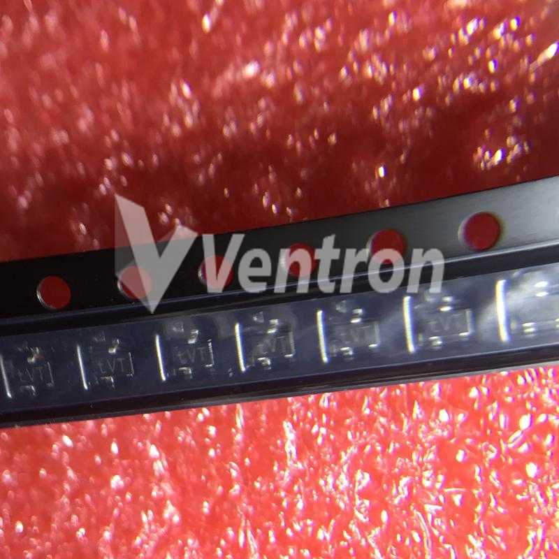
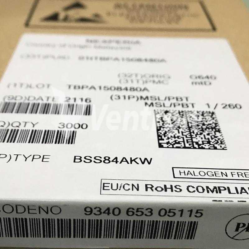
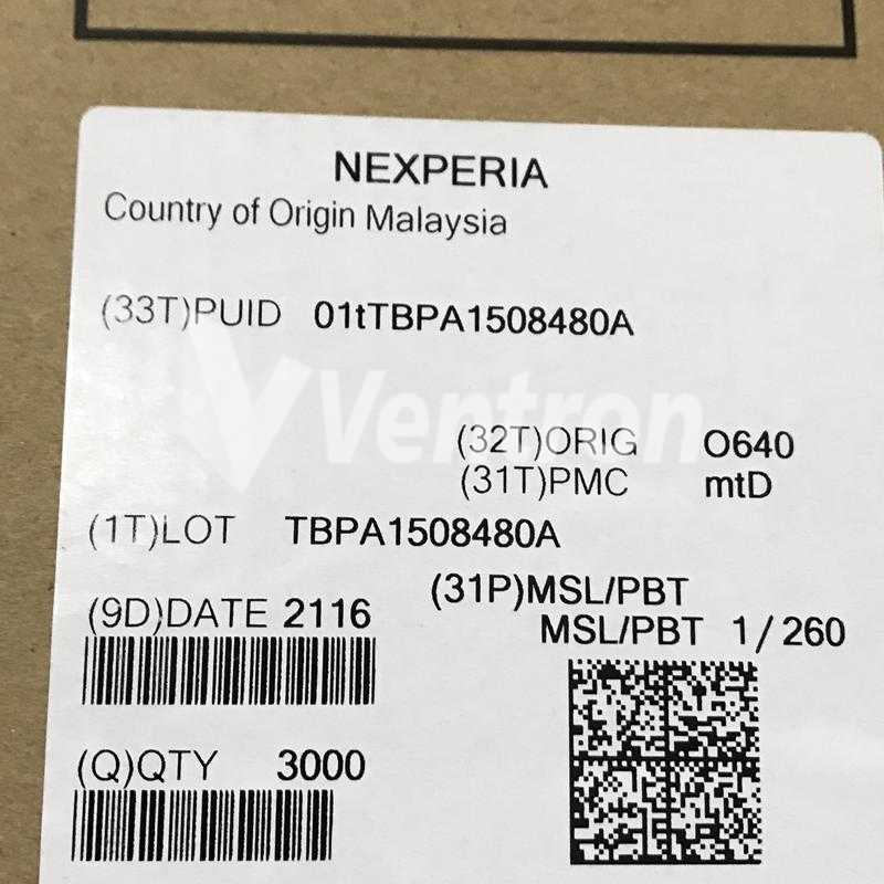
Nexperia USA Inc. BSS84AKW,115
- Part Number:
- BSS84AKW,115
- Manufacturer:
- Nexperia USA Inc.
- Ventron No:
- 3585903-BSS84AKW,115
- Description:
- MOSFET P-CH 50V 150MA SOT323
- ECAD Model:
-
- Datasheet:
- BSS84AKW,115
Nexperia USA Inc. BSS84AKW,115 technical specifications, attributes, parameters and parts with similar specifications to Nexperia USA Inc. BSS84AKW,115.
- Factory Lead Time4 Weeks
- Contact PlatingTin
- Mounting TypeSurface Mount
- Package / CaseSC-70, SOT-323
- Surface MountYES
- Number of Pins3
- Transistor Element MaterialSILICON
- Operating Temperature-55°C~150°C TJ
- PackagingTape & Reel (TR)
- SeriesAutomotive, AEC-Q101, TrenchMOS™
- Published2011
- JESD-609 Codee3
- Part StatusActive
- Moisture Sensitivity Level (MSL)1 (Unlimited)
- Number of Terminations3
- ECCN CodeEAR99
- Resistance7.5Ohm
- Additional FeatureLOGIC LEVEL COMPATIBLE
- TechnologyMOSFET (Metal Oxide)
- Terminal PositionDUAL
- Terminal FormGULL WING
- Pin Count3
- Number of Elements1
- ConfigurationSINGLE WITH BUILT-IN DIODE
- Power Dissipation-Max260mW Ta 830mW Tc
- Operating ModeENHANCEMENT MODE
- Power Dissipation260mW
- Turn On Delay Time13 ns
- FET TypeP-Channel
- Transistor ApplicationSWITCHING
- Rds On (Max) @ Id, Vgs7.5 Ω @ 100mA, 10V
- Vgs(th) (Max) @ Id2.1V @ 250μA
- Input Capacitance (Ciss) (Max) @ Vds36pF @ 25V
- Current - Continuous Drain (Id) @ 25°C150mA Ta
- Gate Charge (Qg) (Max) @ Vgs0.35nC @ 5V
- Rise Time11ns
- Drain to Source Voltage (Vdss)50V
- Drive Voltage (Max Rds On,Min Rds On)10V
- Vgs (Max)±20V
- Fall Time (Typ)25 ns
- Turn-Off Delay Time48 ns
- Continuous Drain Current (ID)150mA
- Gate to Source Voltage (Vgs)20V
- Max Dual Supply Voltage-50V
- Drain to Source Breakdown Voltage-50V
- Radiation HardeningNo
- RoHS StatusROHS3 Compliant
- Lead FreeLead Free
BSS84AKW,115 Overview
As an op amp's input capacitance parameter, CI, is defined as the capacitance between the input terminals when one input is grounded, this device's maximum input capacitance is 36pF @ 25V.This device conducts a continuous drain current (ID) of 150mA, which is the maximum continuous current transistor can conduct.Using VGS=-50V and a specified value of ID, the drain-source breakdown voltage is VDS at which a specified value of ID flows. This device has a drain-source breakdown voltage of -50V (that is, no charge flow from drain to source).When the device is turned off, a turn-off delay time of 48 ns occurs as the input capacitance charges before drain current conduction commences.Before drain current conduction can begin, the device's turning-on delay time takes time to charge its input capacitance. This delay time is 13 ns.Voltage at the gate-source terminal of a FET transistor, called the gate-source voltage, or VGS, can be 20V.With -50V power, it supports a dual voltage supply of up to maximum.This transistor requires a drain-source voltage (Vdss) of 50V.In order to reduce power consumption, this device uses a drive voltage of 10V volts (10V).
BSS84AKW,115 Features
a continuous drain current (ID) of 150mA
a drain-to-source breakdown voltage of -50V voltage
the turn-off delay time is 48 ns
a 50V drain to source voltage (Vdss)
BSS84AKW,115 Applications
There are a lot of Nexperia USA Inc.
BSS84AKW,115 applications of single MOSFETs transistors.
Motor drives and Uninterruptible Power Supplies
Micro Solar Inverter
DC/DC converters
Power Tools
Motor Drives and Uninterruptible Power Supples
Synchronous Rectification
Battery Protection Circuit
Telecom 1 Sever Power Supplies
Industrial Power Supplies
PFC stages, hard switching PWM stages and resonant switching
BSS84AKW,115 More Descriptions
BSS84AKW - 50 V, 150 mA P-channel Trench MOSFET
Trans MOSFET P-CH 50V 0.15A Automotive 3-Pin SC-70 T/R
P-Channel 50 V 7.5 Ohm 260 mW 0.26 nC TrenchMOS FET - SOT-323
Small Signal Field-Effect Transistor, 0.15A I(D), 50V, 1-Element, P-Channel, Silicon, Metal-oxide Semiconductor FET
P CH MOSFET, TRENCH, -50V, -150MA, SOT-323; Transistor Polarity:P Channel; Continuous Drain Current Id:-0.15A; Drain Source Voltage Vds:-50V; On Resistance Rds(on):4.5ohm; Rds(on) Test Voltage Vgs:-10V ;RoHS Compliant: Yes
STANDARD MARKING * REEL PACK, SMD, 7'
NOW NEXPERIA BSS84AKW - SMALL SI
Popular Search Part Number
Related Keywords
Search Tags
Latest News
-
26 March 2024
Everything You Need to Know About the TL431 Voltage Regulator
Ⅰ. What is TL431 regulator?Ⅱ. Main features of TL431Ⅲ. TL431 ratingsⅣ. How to measure the quality of TL431?Ⅴ. What can it be used for?Ⅵ. How to distinguish the... -
26 March 2024
A Complete Guide to the TB6600HG
Ⅰ. TB6600HG descriptionⅡ. Specifications of TB6600HGⅢ. Operating conditions of TB6600HGⅣ. How to connect TB6600HG to the control system?Ⅴ. TB6600HG product featuresⅥ. Pin configuration of TB6600HGⅦ. Function description of... -
27 March 2024
LM358P Op-Amp: Characteristics, Package, Layout, Uses and More
Ⅰ. LM358P descriptionⅡ. Characteristics of LM358PⅢ. Package design of LM358PⅣ. Layout of LM358PⅤ. LM358P usesⅥ. LM358P circuitⅦ. Can LM358 and LM358P be replaced?Ⅷ. How to use LM358P correctly... -
27 March 2024
STM32F030K6T6 Microcontroller Symbol, Characteristics, Specifications and Other Details
Ⅰ. Description of STM32F030K6T6Ⅱ. Functional characteristics of STM32F030K6T6Ⅲ. STM32F030K6T6 specificationsⅣ. Structure of STM32F030K6T6Ⅴ. STM32F030K6T6 symbol, footprint and pin configurationⅥ. STM32F030K6T6 development tools and ecosystemⅦ. Application cases of STM32F030K6T6STM32F030K6T6...

Help you to save your cost and time.
Reliable package for your goods.
Fast Reliable Delivery to save time.
Quality premium after-sale service.