
Fairchild/ON Semiconductor J106
- Part Number:
- J106
- Manufacturer:
- Fairchild/ON Semiconductor
- Ventron No:
- 2495792-J106
- Description:
- JFET N-CH 25V 625MW TO92
- ECAD Model:
-
- Datasheet:
- J105-07, JFTJ105


Fairchild/ON Semiconductor J106 technical specifications, attributes, parameters and parts with similar specifications to Fairchild/ON Semiconductor J106.
- Lifecycle StatusLAST SHIPMENTS (Last Updated: 1 week ago)
- Factory Lead Time7 Weeks
- MountThrough Hole
- Mounting TypeThrough Hole
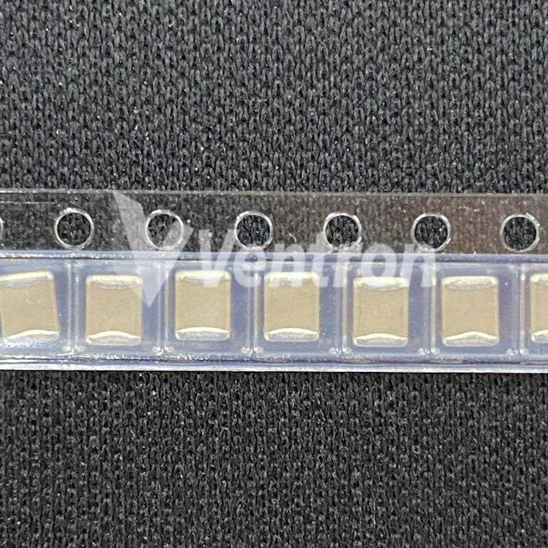
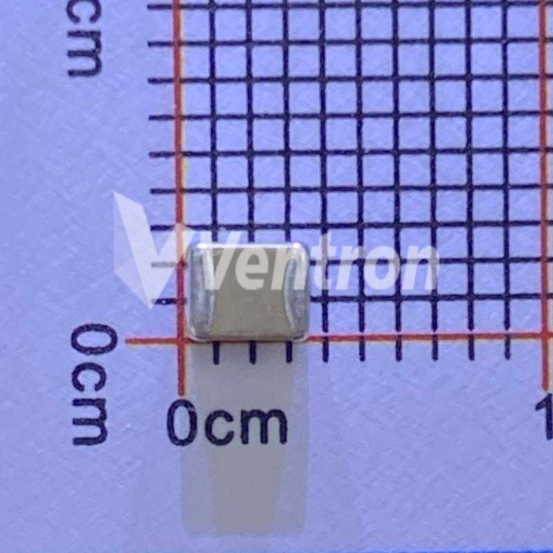
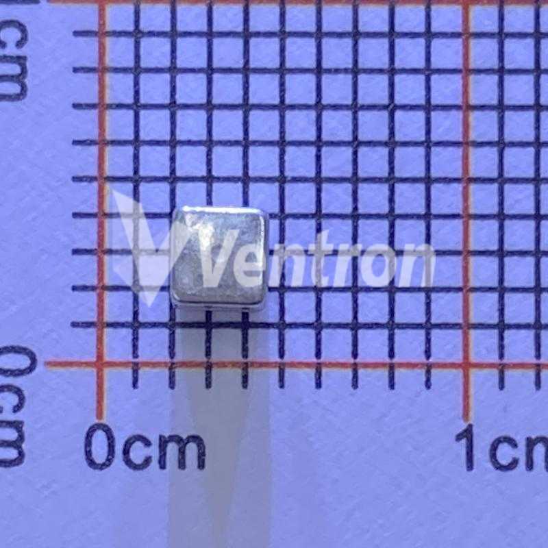
- Package / CaseTO-226-3, TO-92-3 (TO-226AA)
- Number of Pins3
- Weight201mg
- Transistor Element MaterialSILICON
- Operating Temperature-55°C~150°C TJ
- PackagingBulk
- Published2013
- JESD-609 Codee3
- Pbfree Codeyes
- Part StatusObsolete
- Moisture Sensitivity Level (MSL)1 (Unlimited)
- Number of Terminations3
- ECCN CodeEAR99
- Terminal FinishTin (Sn)
- HTS Code8541.21.00.95
- SubcategoryOther Transistors
- Voltage - Rated DC25V
- Max Power Dissipation625mW
- Terminal PositionBOTTOM
- Current Rating200mA
- Number of Elements1
- PolarityNPN
- Element ConfigurationSingle
- Operating ModeDEPLETION MODE
- Power Dissipation625mW
- FET TypeN-Channel
- Transistor ApplicationSWITCHING
- Drain to Source Voltage (Vdss)25V
- Continuous Drain Current (ID)200mA
- Gate to Source Voltage (Vgs)25V
- FET TechnologyJUNCTION
- Drain to Source Resistance6Ohm
- Current - Drain (Idss) @ Vds (Vgs=0)200mA @ 15V
- Voltage - Cutoff (VGS off) @ Id2V @ 1μA
- Resistance - RDS(On)6Ohm
- REACH SVHCNo SVHC
- Radiation HardeningNo
- RoHS StatusROHS3 Compliant
- Lead FreeLead Free
J106 Description
The J106 is an N-channel JFET manufactured by onsemi. The onsemi J106 is designed for analog or digital switching applications where very low ON-resistance is mandatory. Due to the following features, the N-channel JFET J106 can be applied in industrial and power management applications. The J106 is offered in the TO-92 package. It is specified for operation from –55°C to 150°C.
J106 Features
25V Drain-gate voltage
-25V gate-source voltage
10mA Forward gate current
In TO-92-3 package
Operating and Storage Junction Temperature Range: -55 to 150℃
J106 Applications
Body electronics & lighting
Hybrid
electric & powertrain systems
Datacenter & enterprise computing
Mobile phones
PC & notebooks
Portable electronics
Tablets
J106 More Descriptions
J106 Series 25 V 10 mA 6 Ohm N Channel JFET Switch - TO-92
Small Signal Field-Effect Transistor, 1-Element, N-Channel, Silicon, Junction FET, TO-92
JFET, N, TO-92; Transistor Polarity:NPN; Power Dissipation Pd:625mW; Transistor Case Style:TO-92; No. of Pins:3; SVHC:No SVHC (19-Dec-2011); Package / Case:TO-92; Power Dissipation Pd:625mW; Termination Type:Through Hole
N-Channel Switch This device is designed for analog or digital switching applications where very low On Resistance is mandatory. Sourced from Process 59.
Breakdown Voltage Vbr:-25V; Zero Gate Voltage Drain Current Idss Min:200Ma; Zero Gate Voltage Drain Current Idss Max:-; Gate-Source Cutoff Voltage Vgs(Off) Max:-6V; Transistor Type:jfet; No. Of Pins:3 Pin; Product Range:- Rohs Compliant: Yes
Popular Search Part Number
Related Keywords
Search Tags
Latest News
-
18 October 2023
Get to Know the MOC3063 Triac Driver
Ⅰ. What is an optocoupler?Ⅱ. Overview of MOC3063 optocouplerⅢ. Symbol, footprint and pin configuration of MOC3063Ⅳ. Technical parameters of MOC3063Ⅴ. What are the features of MOC3063?Ⅵ. Working principle... -
19 October 2023
TIP122 Darlington Transistor: Symbol, Features, Applications and More
Ⅰ. What is Darlington tube?Ⅱ. Overview of TIP122 transistorⅢ. Symbol and footprint of TIP122 transistorⅣ. Technical parameters of TIP122 transistorⅤ. What are the features of TIP122 transistor?Ⅵ. Pin... -
19 October 2023
LM3900N Quadruple Operational Amplifier: Equivalent, Working Principle and LM3900N vs LM3900DR
Ⅰ. Overview of LM3900NⅡ. Symbol and footprint of LM3900NⅢ. Technical parameters of LM3900NⅣ. What are the features of LM3900N?Ⅴ. Pin configuration of LM3900NⅥ. Circuit and working principle of... -
20 October 2023
TNY268PN Switcher: Symbol, Features, Manufacturer and Applications
Ⅰ. Overview of TNY268PN switcherⅡ. TNY268PN symbol, footprint and pin configurationⅢ. Technical parameters of TNY268PN switcherⅣ. What are the features of TNY268PN switcher?Ⅴ. Manufacturer of TNY268PN switcherⅥ. What...

Help you to save your cost and time.
Reliable package for your goods.
Fast Reliable Delivery to save time.
Quality premium after-sale service.