
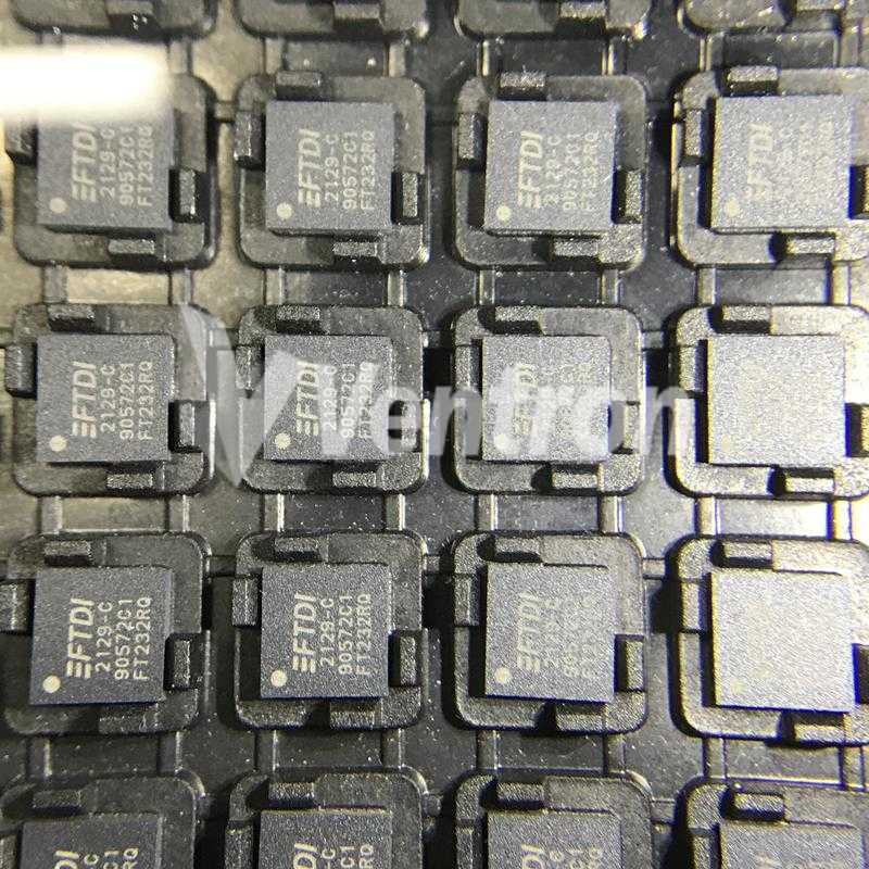
Analog Devices Inc. AD568JQ
- Part Number:
- AD568JQ
- Manufacturer:
- Analog Devices Inc.
- Ventron No:
- 3025200-AD568JQ
- Description:
- IC DAC 12BIT HS MONO 35NS 24CDIP
- ECAD Model:
-
- Datasheet:
- AD568JQ
Analog Devices Inc. AD568JQ technical specifications, attributes, parameters and parts with similar specifications to Analog Devices Inc. AD568JQ.
- Factory Lead Time10 Weeks
- Lifecycle StatusPRODUCTION (Last Updated: 6 days ago)
- Contact PlatingLead, Tin
- MountThrough Hole
- Mounting TypeThrough Hole
- Package / Case24-CDIP (0.300, 7.62mm)
- Number of Pins24
- Operating Temperature0°C~70°C
- PackagingTube
- JESD-609 Codee0
- Pbfree Codeno
- Part StatusActive
- Moisture Sensitivity Level (MSL)1 (Unlimited)
- Number of Terminations24
- ECCN CodeEAR99
- Terminal FinishTin/Lead (Sn63Pb37)
- SubcategoryOther Converters
- Max Power Dissipation100mW
- Terminal PositionDUAL
- Number of Functions1
- Supply Voltage15V
- Terminal Pitch2.54mm
- Base Part NumberAD568
- Pin Count24
- Output TypeCurrent - Unbuffered
- PolarityBipolar, Unipolar
- Max Supply Voltage16.5V
- Min Supply Voltage13.5V
- Nominal Supply Current27mA
- Number of Bits12
- ArchitectureR-2R
- Converter TypeD/A CONVERTER
- Reference TypeInternal
- Data InterfaceParallel
- Differential OutputNo
- Resolution1.5 B
- Voltage - Supply, Analog±13.5V~16.5V
- Voltage - Supply, Digital5V
- Settling Time35μs (Typ)
- Max Dual Supply Voltage16.5V
- Integral Nonlinearity (INL)0.75 LSB
- Min Dual Supply Voltage13.5V
- Input Bit CodeBINARY, OFFSET BINARY
- Dual Supply Voltage15V
- Number of Converters1
- INL/DNL (LSB)±0.75 (Max), ±1 (Max)
- Negative Supply Voltage-Nom-15V
- Height4.572mm
- Length32.77mm
- Width7.493mm
- RoHS StatusNon-RoHS Compliant
- Lead FreeContains Lead
AD568JQ Overview
This product is currently in PRODUCTION and was last updated 6 days ago. The Contact Plating is made of Lead and Tin. The ECCN Code for this product is EAR99. The Supply Voltage is 15V, with a minimum of 13.5V. The Architecture of this product is R-2R and the Reference Type is Internal. The Max Dual Supply Voltage is 16.5V and the Integral Nonlinearity (INL) is 0.75 LSB. This product is Non-RoHS Compliant.
AD568JQ Features
24-CDIP (0.300, 7.62mm) package
24 pin count
24 pins
AD568JQ Applications
There are a lot of Analog Devices Inc. AD568JQ Digital to Analog Converters (DAC)?applications.
Wideband communications:
Voltage Set Point Control
Mobile Communications
Synchro Applications
Data Acquisition
Display Electronics
Instrumentation:
Digitally Controlled Attenuators and Power Supplies
Gain and offset adjustment
Servo controls
AD568JQ More Descriptions
DAC 1-CH R-2R/Current Steering 12-bit 24-Pin CDIP Tube
D/A Converter (D-A) IC; Resolution (Bits):12; Input Channel Type:Parallel; Data Interface:Parallel, CMOS / TTL; Supply Voltage Range:± 13.5V to ± 16.5V; Supply Current:27mA; Digital IC Case Style:DIP; No. of Pins:24 ;RoHS Compliant: No
The AD568 is an ultrahigh-speed, 12-bit digital-to-analog converter (DAC) settling to 0.025% in 35 ns. The monolithic device is fabricated using Analog Devices' Complementary Bipolar (CB) Process. This is a proprietary process featuring high-speed NPN and PNP devices on the same chip without the use of dielectric isolation or multichip hybrid techniques. The high speed of the AD568 is maintained by keeping impedance levels low enough to minimize the effects of parasitic circuit capacitances. The DAC consists of 16 current sources configured to deliver a 10.24 mA full-scale current. Multiple matched current sources and thin-film ladder techniques are combined to produce bit weighting. The DAC's output is a 10.24 mA full scale (FS) for current output applications or a 1.024 V FS unbuffered voltage output. Additionally, a 10.24 V FS buffered output may be generated using an onboard 1 k(ohm) span resistor with an external op amp. Bipolar ranges are accomplished by pin strapping. Laser wafer trimming insures full 12-bit linearity. All grades of the AD568 are guaranteed monotonic over their full operating temperature range. Furthermore, the output resistance of the DAC is trimmed to 100(ohm) =/-1.0%. The gain temperature coefficient of the voltage output is 30 ppm/°C max (K). The AD568 is available in three performance grades. The AD568JQ and KQ are available in 24-pin cerdip (0.3") packages and are specified for operation from 0°C to 70°C. The AD568SQ features operation from -55°C to 125°C and is also packaged in the hermetic 0.3" cerdip.
The three parts on the right have similar specifications to AD568JQ.
-
ImagePart NumberManufacturerFactory Lead TimeLifecycle StatusContact PlatingMountMounting TypePackage / CaseNumber of PinsOperating TemperaturePackagingJESD-609 CodePbfree CodePart StatusMoisture Sensitivity Level (MSL)Number of TerminationsECCN CodeTerminal FinishSubcategoryMax Power DissipationTerminal PositionNumber of FunctionsSupply VoltageTerminal PitchBase Part NumberPin CountOutput TypePolarityMax Supply VoltageMin Supply VoltageNominal Supply CurrentNumber of BitsArchitectureConverter TypeReference TypeData InterfaceDifferential OutputResolutionVoltage - Supply, AnalogVoltage - Supply, DigitalSettling TimeMax Dual Supply VoltageIntegral Nonlinearity (INL)Min Dual Supply VoltageInput Bit CodeDual Supply VoltageNumber of ConvertersINL/DNL (LSB)Negative Supply Voltage-NomHeightLengthWidthRoHS StatusLead FreeSurface MountSeriesTechnologyTerminal FormPeak Reflow Temperature (Cel)Reflow Temperature-Max (s)Power SuppliesInterfacePower DissipationMax Output VoltageMin Input VoltageSlew RateMax Input VoltageSupply TypeSampling RateMin Output VoltageConversion RateDifferential NonlinearityNumber of DAC ChannelsREACH SVHCNumber of D/A ConvertersView Compare
-
 AD568JQ10 WeeksPRODUCTION (Last Updated: 6 days ago)Lead, TinThrough HoleThrough Hole24-CDIP (0.300, 7.62mm)240°C~70°CTubee0noActive1 (Unlimited)24EAR99Tin/Lead (Sn63Pb37)Other Converters100mWDUAL115V2.54mmAD56824Current - UnbufferedBipolar, Unipolar16.5V13.5V27mA12R-2RD/A CONVERTERInternalParallelNo1.5 B±13.5V~16.5V5V35μs (Typ)16.5V0.75 LSB13.5VBINARY, OFFSET BINARY15V1±0.75 (Max), ±1 (Max)-15V4.572mm32.77mm7.493mmNon-RoHS CompliantContains Lead----------------------
 -
14 WeeksPRODUCTION (Last Updated: 1 month ago)Gold-Surface Mount6-TSSOP, SC-88, SOT-3636-40°C~125°CTape & Reel (TR)e4noActive1 (Unlimited)6EAR99-Other Converters500μWDUAL13V-AD56126Voltage - BufferedUnipolar5.5V2.7V-10String DACD/A CONVERTERSupplyI2CNo1.25 B2.7V~5.5V2.7V~5.5V10μs-4 LSB-BINARY-1±4 (Max), ±1 (Max)--2mm-ROHS3 CompliantContains LeadYESnanoDAC®CMOSGULL WING260403/5V2-Wire, I2C, Serial550μW5.5V2.7V0.5 V/μs5.5VSingle1.7 Msps2.7V1.7 Msps----
-
20 WeeksPRODUCTION (Last Updated: 2 weeks ago)Tin-Surface Mount6-WDFN Exposed Pad, CSP6-40°C~125°CTape & Reel (TR)e3noActive1 (Unlimited)6EAR99-Other Converters550μWDUAL13V-AD56016Voltage - BufferedBipolar, Unipolar5.5V2.7V75μA8String DACD/A CONVERTERSupplySPI, DSPNo1 B2.7V~5.5V2.7V~5.5V10μs-0.5 LSB-BINARY--±0.5 (Max), ±0.5 (Max)-750μm2.1mm3.1mmROHS3 CompliantContains LeadYESnanoDAC®CMOS-260303/5VSPI, Serial550μW5.5V2.7V0.5 V/μs5.5VSingle1.7 Msps2.7V1.7 Msps0.5 LSB1No SVHC-
-
----Surface MountDie00°C~70°CTray-noObsolete1 (Unlimited)16EAR99-Other Converters-UPPER15V-AD5610Current - Unbuffered----10R-2RD/A CONVERTERInternalParallelNo-4.5V~16.5V -10.8V~16.5V4.5V~16.5V250ns---BINARY--±0.25, ±0.5-15V---Non-RoHS CompliantContains LeadYES-BIPOLAR-----------------1
Popular Search Part Number
Related Keywords
Search Tags
Latest News
-
08 October 2023
2N3773 Transistor Equivalent, Features and Applications
Ⅰ. 2N3773 transistor overviewⅡ. Symbol and pin connection of 2N3773Ⅲ. Technical parametersⅣ. What are the features of 2N3773?Ⅴ. How does the 2N3773 achieve amplification and switching functions in... -
08 October 2023
IRFP260N Power Mosfet Transistor: Symbol, Features and Working Principle
Ⅰ. IRFP260N transistor descriptionⅡ. Symbol, footprint and pin connection of IRFP260NⅢ. Technical parametersⅣ. Features of IRFP260NⅤ. How does IRFP260N work and how does it drive IRFP260N?Ⅵ. Absolute maximum... -
09 October 2023
TIP117 Darlington Power Transistor Pinout, Equivalent, Features and Uses
Ⅰ. Overview of TIP117Ⅱ. The symbol, footprint and pinout of TIP117Ⅲ. Technical parameters of TIP117Ⅳ. What are the features of TIP117?Ⅴ. Package and packaging of TIP117Ⅵ. What are... -
09 October 2023
Lithium CR2450 Battery Symbol, Equivalent, Specifications and Uses
Ⅰ. What is CR2450 battery?Ⅱ. CR2450 symbol and footprintⅢ. Specifications of CR2450 batteryⅣ. What are the features of CR2450 battery?Ⅴ. What are the uses of CR2450 battery?Ⅵ. What...
Help you to save your cost and time.
Reliable package for your goods.
Fast Reliable Delivery to save time.
Quality premium after-sale service.