
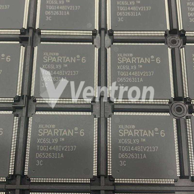
Xilinx Inc. XC6SLX9-3TQG144C
- Part Number:
- XC6SLX9-3TQG144C
- Manufacturer:
- Xilinx Inc.
- Ventron No:
- 3125596-XC6SLX9-3TQG144C
- Description:
- IC FPGA 102 I/O 144TQFP
- ECAD Model:
-
- Datasheet:
- XC6SLX9-3TQG144C
Xilinx Inc. XC6SLX9-3TQG144C technical specifications, attributes, parameters and parts with similar specifications to Xilinx Inc. XC6SLX9-3TQG144C.
- Factory Lead Time10 Weeks
- MountSurface Mount
- Mounting TypeSurface Mount
- Package / Case144-LQFP
- Number of Pins144
- Operating Temperature0°C~85°C TJ
- PackagingTray
- Published2008
- SeriesSpartan®-6 LX
- JESD-609 Codee3
- Pbfree Codeyes
- Part StatusActive
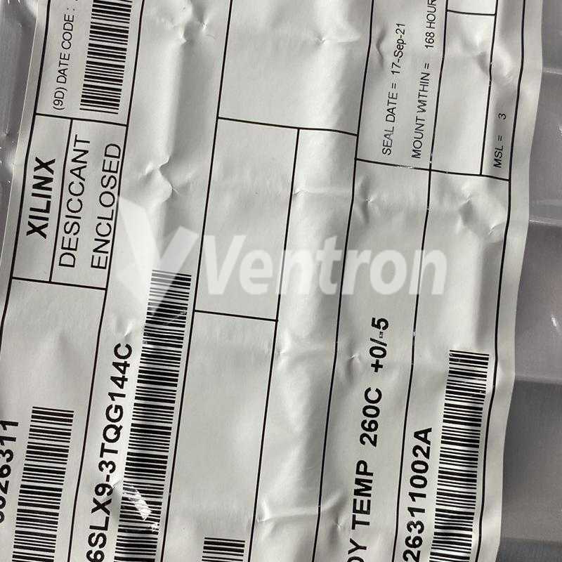
- Moisture Sensitivity Level (MSL)3 (168 Hours)
- Number of Terminations144
- ECCN CodeEAR99
- Terminal FinishMatte Tin (Sn)
- SubcategoryField Programmable Gate Arrays
- TechnologyCMOS
- Voltage - Supply1.14V~1.26V
- Terminal PositionQUAD
- Terminal FormGULL WING
- Peak Reflow Temperature (Cel)260
- Supply Voltage1.2V
- Terminal Pitch0.5mm
- Reflow Temperature-Max (s)30
- Base Part NumberXC6SLX9
- Pin Count144
- Number of Outputs102
- Qualification StatusNot Qualified
- Operating Supply Voltage1.2V
- Number of I/O102
- RAM Size72kB
- Clock Frequency862MHz
- Programmable Logic TypeFIELD PROGRAMMABLE GATE ARRAY
- Number of Logic Elements/Cells9152
- Total RAM Bits589824
- Number of LABs/CLBs715
- Speed Grade3
- Number of Registers11440
- Combinatorial Delay of a CLB-Max0.21 ns
- Number of CLBs715
- Height Seated (Max)1.6mm
- Length20mm
- Width20mm
- RoHS StatusROHS3 Compliant
XC6SLX9-3TQG144C Overview
The package or case for this particular device is a 144-LQFP, which stands for Low Profile Quad Flat Package. This package is commonly used for integrated circuits and provides a compact and efficient design. The operating temperature for this device is 0°C to 85°C, which is a wide range that allows for reliable operation in various environments. The JESD-609 code for this device is e3, indicating that it meets the industry standards for electrostatic discharge sensitivity. The terminal position is QUAD, meaning that the pins are arranged in a square pattern. With a supply voltage of 1.2V, this device is able to operate efficiently while consuming minimal power. The reflow temperature-max (s) is 30, indicating the maximum temperature that the device can withstand during the soldering process. This device also boasts an impressive number of LABs/CLBs, with 715 available for use. The speed grade of 3 ensures fast and efficient performance, while the number of registers, which is 11440, allows for a high level of customization and control. With a width of 20mm, this device offers a compact yet powerful solution for various electronic designs.
XC6SLX9-3TQG144C Features
102 I/Os
Up to 589824 RAM bits
144 LABs/CLBs
11440 registers
XC6SLX9-3TQG144C Applications
There are a lot of Xilinx Inc. XC6SLX9-3TQG144C FPGAs applications.
ASIC prototyping
Aircraft navigation
Cryptography
Software-defined radios
Device controllers
Automotive advanced driver assistance systems (ADAS)
Defense Applications
Aerospace and Defense
Data Center
Security systems
XC6SLX9-3TQG144C More Descriptions
FPGA Spartan-6 LX Family 9152 Cells 45nm (CMOS) Technology 1.2V 144-Pin TQFP
Spartan-6 FPGA, 200 Max User I/O, Speed Grade-3, Logic Cells 9152, TQG144, RoHSXilinx SCT
Field Programmable Gate Array, 715 CLBs, 862MHz, 9152-Cell, CMOS, PQFP144
XILINX XC6SLX9-3TQG144C / IC FPGA 102 I/O 144TQFP
FPGA - Field Programmable Gate Array XC6SLX9-3TQG144C
Product Description Demo for Development.
French Electronic Distributor since 1988
The three parts on the right have similar specifications to XC6SLX9-3TQG144C.
-
ImagePart NumberManufacturerFactory Lead TimeMountMounting TypePackage / CaseNumber of PinsOperating TemperaturePackagingPublishedSeriesJESD-609 CodePbfree CodePart StatusMoisture Sensitivity Level (MSL)Number of TerminationsECCN CodeTerminal FinishSubcategoryTechnologyVoltage - SupplyTerminal PositionTerminal FormPeak Reflow Temperature (Cel)Supply VoltageTerminal PitchReflow Temperature-Max (s)Base Part NumberPin CountNumber of OutputsQualification StatusOperating Supply VoltageNumber of I/ORAM SizeClock FrequencyProgrammable Logic TypeNumber of Logic Elements/CellsTotal RAM BitsNumber of LABs/CLBsSpeed GradeNumber of RegistersCombinatorial Delay of a CLB-MaxNumber of CLBsHeight Seated (Max)LengthWidthRoHS StatusHTS CodePower SuppliesReach Compliance CodeTime@Peak Reflow Temperature-Max (s)Surface MountJESD-30 CodeNumber of InputsView Compare
-
 XC6SLX9-3TQG144C10 WeeksSurface MountSurface Mount144-LQFP1440°C~85°C TJTray2008Spartan®-6 LXe3yesActive3 (168 Hours)144EAR99Matte Tin (Sn)Field Programmable Gate ArraysCMOS1.14V~1.26VQUADGULL WING2601.2V0.5mm30XC6SLX9144102Not Qualified1.2V10272kB862MHzFIELD PROGRAMMABLE GATE ARRAY91525898247153114400.21 ns7151.6mm20mm20mmROHS3 Compliant--------
 -
10 WeeksSurface MountSurface Mount256-LBGA2560°C~85°C TJTray2008Spartan®-6 LXe1yesActive3 (168 Hours)256EAR99Tin/Silver/Copper (Sn96.5Ag3.0Cu0.5)Field Programmable Gate ArraysCMOS1.14V~1.26VBOTTOMBALL2601V1mm30XC6SLX9256186Not Qualified1V18672kB-FIELD PROGRAMMABLE GATE ARRAY9152589824715-114400.46 ns7151.55mm17mm17mmROHS3 Compliant8542.39.00.0112.5/3.3V-----
-
10 WeeksSurface MountSurface Mount256-LBGA2560°C~85°C TJTray2008Spartan®-6 LXe0noActive3 (168 Hours)256EAR99Tin/Lead (Sn63Pb37)Field Programmable Gate ArraysCMOS1.14V~1.26VBOTTOMBALL2401.2V1mm-XC6SLX16256186Not Qualified1.2V18672kB667MHzFIELD PROGRAMMABLE GATE ARRAY145795898241139218224--1.55mm17mm17mmNon-RoHS Compliant--not_compliant30---
-
--Surface Mount484-BBGA-0°C~85°C TJTray2008Spartan®-6 LXTe0-Obsolete3 (168 Hours)4843A991.DTin/Lead (Sn63Pb37)Field Programmable Gate ArraysCMOS1.14V~1.26VBOTTOMBALL2251.2V1mm-XC6SLX150-296Not Qualified-296-806MHzFIELD PROGRAMMABLE GATE ARRAY147443493977611519--0.26 ns-2.6mm23mm23mmNon-RoHS Compliant8542.39.00.011.21.2/3.32.5/3.3V-30YESS-PBGA-B484296

Popular Search Part Number
Related Keywords
Search Tags
Latest News
-
27 March 2024
STM32F030K6T6 Microcontroller Symbol, Characteristics, Specifications and Other Details
Ⅰ. Description of STM32F030K6T6Ⅱ. Functional characteristics of STM32F030K6T6Ⅲ. STM32F030K6T6 specificationsⅣ. Structure of STM32F030K6T6Ⅴ. STM32F030K6T6 symbol, footprint and pin configurationⅥ. STM32F030K6T6 development tools and ecosystemⅦ. Application cases of STM32F030K6T6STM32F030K6T6... -
28 March 2024
An Introduction to TPS54302DDCR Synchronous Buck Converter
Ⅰ. What is TPS54302DDCR?Ⅱ. Characteristics of TPS54302DDCRⅢ. Simplified schematic of TPS54302DDCRⅣ. What are the advantages of TPS54302DDCR?Ⅴ. Technical parameters of TPS54302DDCRⅥ. Pin configuration and functions of TPS54302DDCRⅦ. Protection... -
28 March 2024
UCC27517DBVR Gate Driver: Replacements, Advantages, Application and Package
Ⅰ. UCC27517DBVR overviewⅡ. Technical parameters of UCC27517DBVRⅢ. UCC27517DBVR's typical characteristicsⅣ. What are the advantages of UCC27517DBVR compared with other gate driver ICs?Ⅴ. What applications is the UCC27517DBVR typically... -
29 March 2024
TLP2362 Optocoupler Characteristics, Specifications, Working Principle and More
Ⅰ. Overview of TLP2362Ⅱ. Characteristics of TLP2362Ⅲ. Specifications of TLP2362Ⅳ. Recommended operating conditions of TLP2362Ⅴ. How does TLP2362 work?Ⅵ. Internal equivalent circuit of TLP2362Ⅶ. Storage and soldering of...
Help you to save your cost and time.
Reliable package for your goods.
Fast Reliable Delivery to save time.
Quality premium after-sale service.