
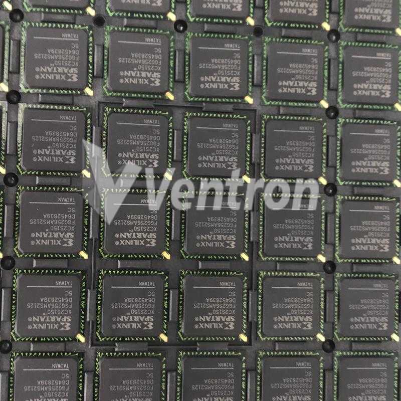
Xilinx Inc. XC2S150-5FGG256C
- Part Number:
- XC2S150-5FGG256C
- Manufacturer:
- Xilinx Inc.
- Ventron No:
- 3126384-XC2S150-5FGG256C
- Description:
- IC FPGA 176 I/O 256FBGA
- ECAD Model:
-
- Datasheet:
- XC2S150-5FGG256C


Xilinx Inc. XC2S150-5FGG256C technical specifications, attributes, parameters and parts with similar specifications to Xilinx Inc. XC2S150-5FGG256C.
- Factory Lead Time10 Weeks
- MountSurface Mount
- Mounting TypeSurface Mount
- Package / Case256-BGA
- Number of Pins256
- Operating Temperature0°C~85°C TJ
- PackagingTray
- Published2004
- SeriesSpartan®-II
- JESD-609 Codee1
- Pbfree Codeyes
- Part StatusActive
- Moisture Sensitivity Level (MSL)3 (168 Hours)
- Number of Terminations256
- ECCN CodeEAR99
- SubcategoryField Programmable Gate Arrays
- TechnologyCMOS
- Voltage - Supply2.375V~2.625V
- Terminal PositionBOTTOM
- Terminal FormBALL
- Peak Reflow Temperature (Cel)260
- Supply Voltage2.5V
- Terminal Pitch1mm
- Reflow Temperature-Max (s)30
- Base Part NumberXC2S150
- Pin Count256
- Number of Outputs260
- Qualification StatusNot Qualified
- Operating Supply Voltage2.5V
- Number of I/O176
- RAM Size6kB
- Clock Frequency263MHz
- Programmable Logic TypeFIELD PROGRAMMABLE GATE ARRAY
- Number of Logic Elements/Cells3888
- Total RAM Bits49152
- Number of Gates150000
- Number of LABs/CLBs864
- Speed Grade5
- Combinatorial Delay of a CLB-Max0.7 ns
- Number of CLBs864
- Height Seated (Max)2mm
- Length17mm
- Width17mm
- RoHS StatusROHS3 Compliant
- Lead FreeLead Free
XC2S150-5FGG256C Overview
The manufacturer of this component is Xilinx Inc. It is a type of chip called Embedded - FPGAs (Field Programmable Gate Array), which falls under the category of Embedded - FPGAs (Field Programmable Gate Array). The package or case size is 256-BGA and it has 256 pins. The ECCN code assigned to it is EAR99, and its supply voltage is 2.5V. It has a total of 176 input/output connections, and a RAM size of 6kB. The clock frequency of this chip is 263MHz, and its speed grade is 5. The maximum combinational delay of a CLB (Configurable Logic Block) is 0.7 nanoseconds. This component is also compliant with the RoHS (Restriction of Hazardous Substances) directive, meeting the requirements of the third version.
XC2S150-5FGG256C Features
176 I/Os
Up to 49152 RAM bits
256 LABs/CLBs
XC2S150-5FGG256C Applications
There are a lot of Xilinx Inc. XC2S150-5FGG256C FPGAs applications.
Server Applications
Image processing
Electronic Warfare
OpenCL
Automotive Applications
Cryptography
Integrating multiple SPLDs
Telecommunication
Space Applications
Secure Communication
XC2S150-5FGG256C More Descriptions
FPGA Spartan-II Family 150K Gates 3888 Cells 263MHz 0.18um Technology 2.5V 256-Pin FBGA
Field Programmable Gate Array, 864 CLBs, 52000 Gates, 357MHz, 3888-Cell, CMOS, PBGA256
BGA-256 Programmable Logic Device (CPLDs/FPGAs) ROHS
Product Description Demo for Development.
Field Programmable Gate Array, 864 CLBs, 52000 Gates, 357MHz, 3888-Cell, CMOS, PBGA256
BGA-256 Programmable Logic Device (CPLDs/FPGAs) ROHS
Product Description Demo for Development.
Popular Search Part Number
Related Keywords
Search Tags
Latest News
-
19 March 2024
HT1621B Alternatives, Brand, Usage and Other Details
Ⅰ. Overview of HT1621BⅡ. Which brand is HT1621B?Ⅲ. Pins and description of HT1621BⅣ. How to use HT1621B?Ⅴ. Application circuits of HT1621BⅥ. Tips for using HT1621BⅦ. How to set... -
19 March 2024
AT24C02 Pinout, Working Principle, Characteristics and More
Ⅰ. AT24C02 overviewⅡ. Working principle of AT24C02Ⅲ. Pins and functions of AT24C02Ⅳ. Characteristics of AT24C02Ⅴ. Block diagram of AT24C02Ⅵ. What should we pay attention to when using AT24C02?Ⅶ.... -
20 March 2024
L9110S Advantages, Pinout, Working Principle and Application
Ⅰ. L9110S overviewⅡ. Advantages of L9110SⅢ. L9110S pin configurationⅣ. Hardware introduction of L9110S motor drive moduleⅤ. Working principle of L9110S motor drive moduleⅥ. L9110S application circuitⅦ. How to... -
20 March 2024
PCF8563 Alternatives, Characteristics, Functions and More
Ⅰ. Introduction to PCF8563Ⅱ. Characteristics of PCF8563Ⅲ. Main functions of PCF8563Ⅳ. Block diagram of PCF8563Ⅴ. How does PCF8563 work?Ⅵ. Application circuit of PCF8563Ⅶ. Limiting values of PCF8563Ⅷ. How...

Help you to save your cost and time.
Reliable package for your goods.
Fast Reliable Delivery to save time.
Quality premium after-sale service.