
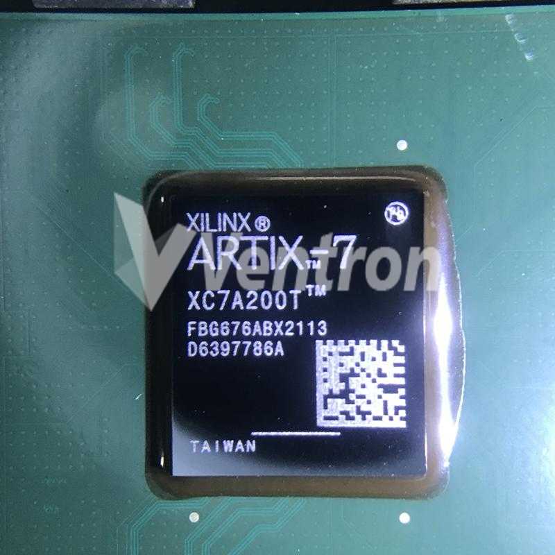
Xilinx Inc. XC7A200T-2FBG676C
- Part Number:
- XC7A200T-2FBG676C
- Manufacturer:
- Xilinx Inc.
- Ventron No:
- 3125655-XC7A200T-2FBG676C
- Description:
- IC FPGA ARTIX7 400 I/O 676FCBGA
- ECAD Model:
-
- Datasheet:
- XC7A200T-2FBG676C
Xilinx Inc. XC7A200T-2FBG676C technical specifications, attributes, parameters and parts with similar specifications to Xilinx Inc. XC7A200T-2FBG676C.
- Factory Lead Time10 Weeks
- Contact PlatingCopper, Silver, Tin
- Mounting TypeSurface Mount
- Package / Case676-BBGA, FCBGA
- Surface MountYES
- Number of Pins676
- Operating Temperature0°C~85°C TJ
- PackagingTray
- Published2009
- SeriesArtix-7
- JESD-609 Codee1
- Pbfree Codeyes
- Part StatusActive
- Moisture Sensitivity Level (MSL)4 (72 Hours)
- Number of Terminations676
- ECCN Code3A991.D
- Terminal FinishTin/Silver/Copper (Sn96.5Ag3.0Cu0.5)
- HTS Code8542.39.00.01
- SubcategoryField Programmable Gate Arrays
- TechnologyCMOS
- Voltage - Supply0.95V~1.05V
- Terminal PositionBOTTOM
- Terminal FormBALL
- Peak Reflow Temperature (Cel)NOT SPECIFIED
- Supply Voltage1V
- Terminal Pitch1mm
- Reflow Temperature-Max (s)NOT SPECIFIED
- Base Part NumberXC7A200T
- Pin Count676
- Number of Outputs400
- Qualification StatusNot Qualified
- Power Supplies1V
- Memory Size1GB
- Number of I/O400
- RAM Size1.6MB
- Memory TypeDDR3
- Clock Frequency1286MHz
- Programmable Logic TypeFIELD PROGRAMMABLE GATE ARRAY
- Number of Logic Elements/Cells215360
- Total RAM Bits13455360
- Number of LABs/CLBs16825
- Speed Grade-2
- Number of Registers269200
- Combinatorial Delay of a CLB-Max1.05 ns
- Height Seated (Max)2.54mm
- Length27mm
- Width27mm
- RoHS StatusROHS3 Compliant
XC7A200T-2FBG676C Overview
There is a 676-BBGA, FCBGA package that includes this component. There are FIELD PROGRAMMABLE GATE ARRAY transistors in this type of FPGA. Its 400 I/Os help it transfer data more efficiently. Logic elements/cells form the fundamental building block of a computer. It is powered from a supply voltage of 1V. Field Programmable Gate Arrays family FPGA part. By attaching the Surface Mount connector, you can use this FPGA module with your development board. Fpga chips operates at a voltage of 0.95V~1.05V and uses a battery to supply power. The FPGA belongs to the Artix-7 series of FPGAs, and it is one type of FPGA. While operating, the operating temperature should be kept within a range of 0°C~85°C TJ. This device is equipped with 400 separate outputs, which makes it a very versatile device. There is an FPGA model contained in Tray in order to conserve space. In total, it has a total of 676 terminations. Having a RAM bit size of 13455360 means that this device will offer you a lot of memory. You can find related parts by using the part number XC7A200T, which is its base part number. The FPGA module's RAM si1.6MBe reaches 1.6MB in order to ensure that the program operates in a normal manner. In order to make it work, 676 pins have been designed. The FPGA is built as an array of 16825 latches or CLBs. There is a 1V power supply that is required to operate it. I am going to present you with a device that is equipped with 676 pins. Most commonly, this device makes use of an oscillating crystal frequency of 1286MHz to operate. For storing programs and data, this FPGA module embeds memory 1GB. A total of 269200 registers are used for storing and transferring data between them. A DDR3 memory provides data storage and avoids resource conflicts.
XC7A200T-2FBG676C Features
400 I/Os
Up to 13455360 RAM bits
676 LABs/CLBs
269200 registers
XC7A200T-2FBG676C Applications
There are a lot of Xilinx Inc. XC7A200T-2FBG676C FPGAs applications.
Military DSP
Embedded Vision
Aerospace and Defense
Radar and Sensors
Data Mining
Filtering and communication encoding
Industrial Ethernet
High Performance Computing
Scientific Instruments
Voice recognition
XC7A200T-2FBG676C More Descriptions
Artix-7 FPGA, 400 User I/Os, 8 GTP, 676-Ball BGA, Speed Grade 2, Commercial Grade, FBG676, RoHSXilinx SCT
FPGA Artix-7 Family 215360 Cells 28nm Technology 1V 676-Pin Lidless FCBGA
Field Programmable Gate Array, 16825 CLBs, 1286MHz, 215360-Cell, CMOS, PBGA676
Artix-7 XC7A200T 676-BBGA FCBGA Tin/Silver/Copper (Sn96.5Ag3.0Cu0.5) field programmable gate array 2.54mm 1V 1286MHz 1.05ns
FPGA, ARTIX-7, 400 I/O, FCBGA-676; No. of Logic Blocks:33650; No. of Macrocells:215360Macrocells; FPGA Family:Artix-7; Logic Case Style:FCBGA; No. of Pins:676Pins; No. of Speed Grades:2; Total RAM Bits:13140Kbit; MSL:- RoHS Compliant: Yes
The three parts on the right have similar specifications to XC7A200T-2FBG676C.
-
ImagePart NumberManufacturerFactory Lead TimeContact PlatingMounting TypePackage / CaseSurface MountNumber of PinsOperating TemperaturePackagingPublishedSeriesJESD-609 CodePbfree CodePart StatusMoisture Sensitivity Level (MSL)Number of TerminationsECCN CodeTerminal FinishHTS CodeSubcategoryTechnologyVoltage - SupplyTerminal PositionTerminal FormPeak Reflow Temperature (Cel)Supply VoltageTerminal PitchReflow Temperature-Max (s)Base Part NumberPin CountNumber of OutputsQualification StatusPower SuppliesMemory SizeNumber of I/ORAM SizeMemory TypeClock FrequencyProgrammable Logic TypeNumber of Logic Elements/CellsTotal RAM BitsNumber of LABs/CLBsSpeed GradeNumber of RegistersCombinatorial Delay of a CLB-MaxHeight Seated (Max)LengthWidthRoHS StatusMountPropagation DelayTurn On Delay TimeSupplier Device PackageMax Operating TemperatureMin Operating TemperatureNumber of Logic Blocks (LABs)View Compare
-
 XC7A200T-2FBG676C10 WeeksCopper, Silver, TinSurface Mount676-BBGA, FCBGAYES6760°C~85°C TJTray2009Artix-7e1yesActive4 (72 Hours)6763A991.DTin/Silver/Copper (Sn96.5Ag3.0Cu0.5)8542.39.00.01Field Programmable Gate ArraysCMOS0.95V~1.05VBOTTOMBALLNOT SPECIFIED1V1mmNOT SPECIFIEDXC7A200T676400Not Qualified1V1GB4001.6MBDDR31286MHzFIELD PROGRAMMABLE GATE ARRAY2153601345536016825-22692001.05 ns2.54mm27mm27mmROHS3 Compliant--------
 -
10 WeeksCopper, Silver, TinSurface Mount256-LBGA-2560°C~85°C TJTray2010Artix-7e1yesActive3 (168 Hours)256EAR99Tin/Silver/Copper (Sn/Ag/Cu)-Field Programmable Gate ArraysCMOS0.95V~1.05VBOTTOMBALLNOT SPECIFIED1V-NOT SPECIFIED-256170Not Qualified1V-170337.5kB--FIELD PROGRAMMABLE GATE ARRAY5216027648004075165200----ROHS3 CompliantSurface Mount1.09 ns1.09 ns----
-
--Surface Mount324-LFBGA, CSPBGA--0°C~85°C TJTray2009Artix-7--Obsolete3 (168 Hours)------0.95V~1.05V------XC7A100T-----210607.5kB---10144049766407925------RoHS CompliantSurface Mount--324-CSPBGA (15x15)85°C0°C7925
-
12 WeeksCopper, Silver, TinSurface Mount484-BBGA-4840°C~100°C TJTray2010Artix-7e1yesActive4 (72 Hours)484---Field Programmable Gate ArraysCMOS0.95V~1.05VBOTTOMBALLNOT SPECIFIED1V1mmNOT SPECIFIED-484285Not Qualified1V-285472.5kB-1412MHzFIELD PROGRAMMABLE GATE ARRAY75520387072059003944000.94 ns2.6mm--ROHS3 CompliantSurface Mount810 ps810 ps----
Popular Search Part Number
Related Keywords
Search Tags
Latest News
-
27 November 2023
TL082 Operational Amplifier Equivalents, Features, TL072 vs TL082 and Applications
Ⅰ. Overview of TL082 operational amplifierⅡ. Features of TL082 operational amplifierⅢ. Pin configuration of TL082 operational amplifierⅣ. How does the output short-circuit protection function of TL082 work?Ⅴ. Functional... -
27 November 2023
BT151 SCR Features, Pin Configuration, Working Principle and Applications
Ⅰ. What is a one-way thyristor?Ⅱ. Overview of BT151Ⅲ. What are the features of BT151?Ⅳ. Footprint and pin configuration of BT151Ⅴ. Technical parameters of BT151Ⅵ. How to measure... -
28 November 2023
An Introduction to LM393 Low Power Dual Voltage Comparator
Ⅰ. What is LM393 comparator?Ⅱ. What are the features of LM393 comparator?Ⅲ. Pin configuration of LM393 comparatorⅣ. Functions of LM393 comparatorⅤ. Technical parameters of LM393 comparatorⅥ. Typical circuit... -
28 November 2023
Get to Know the TL494 Pulse-Width-Modulation Control Circuits
Ⅰ. Overview of TL494Ⅱ. What are the features of TL494?Ⅲ. TL494 symbol, footprint and pin configurationⅣ. Internal structure and working parts of TL494Ⅴ. How does the TL494 work?Ⅵ....
Help you to save your cost and time.
Reliable package for your goods.
Fast Reliable Delivery to save time.
Quality premium after-sale service.