
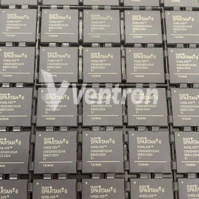
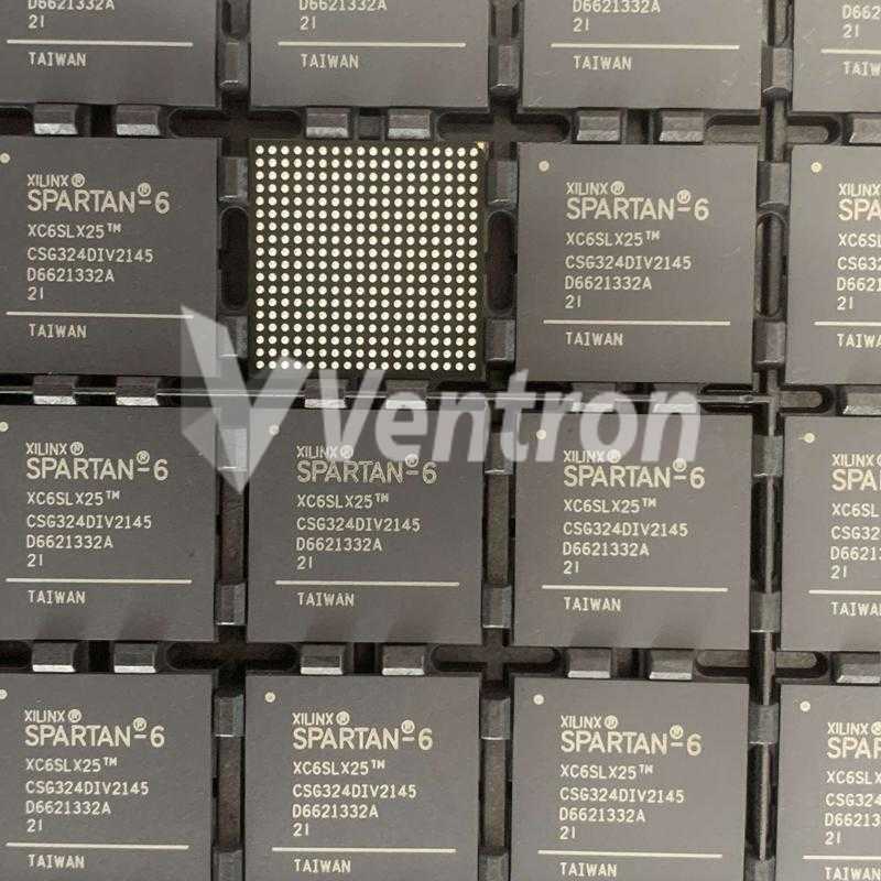
Xilinx Inc. XC6SLX25-2CSG324I
- Part Number:
- XC6SLX25-2CSG324I
- Manufacturer:
- Xilinx Inc.
- Ventron No:
- 3632194-XC6SLX25-2CSG324I
- Description:
- IC FPGA 226 I/O 324CSBGA
- ECAD Model:
-
- Datasheet:
- XC6SLX25-2CSG324I


Xilinx Inc. XC6SLX25-2CSG324I technical specifications, attributes, parameters and parts with similar specifications to Xilinx Inc. XC6SLX25-2CSG324I.
- Factory Lead Time10 Weeks
- Contact PlatingCopper, Silver, Tin
- MountSurface Mount
- Mounting TypeSurface Mount
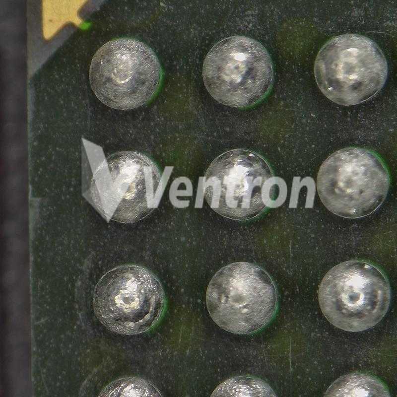
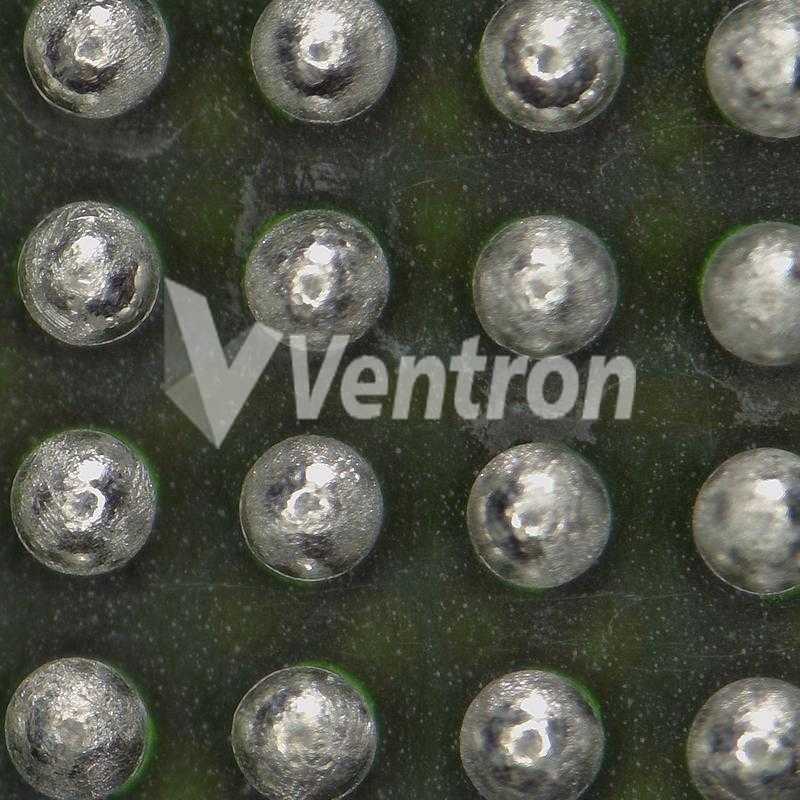
- Package / Case324-LFBGA, CSPBGA
- Number of Pins324
- Operating Temperature-40°C~100°C TJ
- PackagingTray
- Published2008
- SeriesSpartan®-6 LX
- JESD-609 Codee1
- Pbfree Codeyes
- Part StatusActive
- Moisture Sensitivity Level (MSL)3 (168 Hours)
- Number of Terminations324
- ECCN Code3A991.D
- Terminal FinishTin/Silver/Copper (Sn96.5Ag3.0Cu0.5)
- SubcategoryField Programmable Gate Arrays
- TechnologyCMOS
- Voltage - Supply1.14V~1.26V
- Terminal PositionBOTTOM
- Terminal FormBALL
- Peak Reflow Temperature (Cel)260
- Supply Voltage1.2V
- Terminal Pitch0.8mm
- Reflow Temperature-Max (s)30
- Base Part NumberXC6SLX25
- Pin Count324
- Number of Outputs226
- Qualification StatusNot Qualified
- Operating Supply Voltage1.2V
- Number of I/O226
- RAM Size117kB
- Clock Frequency667MHz
- Programmable Logic TypeFIELD PROGRAMMABLE GATE ARRAY
- Number of Logic Elements/Cells24051
- Total RAM Bits958464
- Number of LABs/CLBs1879
- Speed Grade2
- Number of Registers30064
- Height Seated (Max)1.5mm
- Length15mm
- Width15mm
- REACH SVHCUnknown
- RoHS StatusROHS3 Compliant
XC6SLX25-2CSG324I Overview
As part of the 324-LFBGA, CSPBGA package, it is included. In this kind of FPGA, FIELD PROGRAMMABLE GATE ARRAY is used. 226 I/Os are available for transferring data more efficiently. The basic building blocks of logic contain 24051 logic elements/cells. It is powered from a supply voltage of 1.2V. The Field Programmable Gate Arrays family of FPGAs includes this part. The Surface Mount-slot connector on the FPGA module can be connected to the development board. In order to operate it, it requires a voltage supply of 1.14V~1.26V . There are many types of FPGAs in the Spartan?-6 LX series, this is one of them. Fpga chips is important to maintain the operating temperature wFpga chipshin the range of -40°C~100°C TJ when operating the machine. A total of 226 outputs are incorporated into this device. Using the Tray layout, this FPGA model can be contained in a very small amount of space. In total, it has a total of 324 terminations. There are 958464 RAM bits that are available with this device. You can find related parts by using the part number XC6SLX25, which is its base part number. Fpga electronics is important that this FPGA module has a RAM si117kBe of 117kB in order to ensure that the program will run normally. In order to make it work, 324 pins have been designed. A total of 1879 LABs/CLBs are included in this FPGA. As long as this FPGA is mounted in Surface Mount, it should be able to function as it should in terms of its specifications, as well as its capabilities. In operation with 1.2V, designers can take advantage of its flexibility to the fullest extent. This device has a pin count of 324 in fpga semiconductor. Usually, fpga semiconductor uses a 667MHz crystal. The data is stored and transferred using 30064 registers that are used for this purpose.
XC6SLX25-2CSG324I Features
226 I/Os
Up to 958464 RAM bits
324 LABs/CLBs
30064 registers
XC6SLX25-2CSG324I Applications
There are a lot of Xilinx Inc. XC6SLX25-2CSG324I FPGAs applications.
Secure Communication
ASIC prototyping
Security systems
Voice recognition
Integrating multiple SPLDs
Aerospace and Defense
Defense Applications
Wired Communications
Computer hardware emulation
Automotive Applications
XC6SLX25-2CSG324I More Descriptions
FPGA Spartan-6 LX Family 24051 Cells 45nm (CMOS) Technology 1.2V 324-Pin CS-BGA
Field Programmable Gate Array, 1879 CLBs, 667MHz, 24051-Cell, CMOS, PBGA324
FPGA, SPARTAN-6, 226 I/O, CSBGA-324; No. of Logic Cells:24051Logic Cells; IC Case / Package:CSBGA; No. of Pins:324Pins; No.of User I/Os:226I/O s; Product Range:Spartan-6 XC6SLX25 Series; MSL:-; Clock Management:DCM, PLL RoHS Compliant: Yes
The three parts on the right have similar specifications to XC6SLX25-2CSG324I.
-
ImagePart NumberManufacturerFactory Lead TimeContact PlatingMountMounting TypePackage / CaseNumber of PinsOperating TemperaturePackagingPublishedSeriesJESD-609 CodePbfree CodePart StatusMoisture Sensitivity Level (MSL)Number of TerminationsECCN CodeTerminal FinishSubcategoryTechnologyVoltage - SupplyTerminal PositionTerminal FormPeak Reflow Temperature (Cel)Supply VoltageTerminal PitchReflow Temperature-Max (s)Base Part NumberPin CountNumber of OutputsQualification StatusOperating Supply VoltageNumber of I/ORAM SizeClock FrequencyProgrammable Logic TypeNumber of Logic Elements/CellsTotal RAM BitsNumber of LABs/CLBsSpeed GradeNumber of RegistersHeight Seated (Max)LengthWidthREACH SVHCRoHS StatusSurface MountHTS CodeReach Compliance CodeTime@Peak Reflow Temperature-Max (s)JESD-30 CodePower SuppliesNumber of InputsCombinatorial Delay of a CLB-MaxView Compare
-
 XC6SLX25-2CSG324I10 WeeksCopper, Silver, TinSurface MountSurface Mount324-LFBGA, CSPBGA324-40°C~100°C TJTray2008Spartan®-6 LXe1yesActive3 (168 Hours)3243A991.DTin/Silver/Copper (Sn96.5Ag3.0Cu0.5)Field Programmable Gate ArraysCMOS1.14V~1.26VBOTTOMBALL2601.2V0.8mm30XC6SLX25324226Not Qualified1.2V226117kB667MHzFIELD PROGRAMMABLE GATE ARRAY2405195846418792300641.5mm15mm15mmUnknownROHS3 Compliant---------
 -
---Surface Mount256-LBGA--40°C~100°C TJTray2008Spartan®-6 LXe0-Obsolete3 (168 Hours)256EAR99Tin/Lead (Sn63Pb37)Field Programmable Gate ArraysCMOS1.14V~1.26VBOTTOMBALL2401.2V1mm-XC6SLX16-186Not Qualified-186-806MHzFIELD PROGRAMMABLE GATE ARRAY145795898241139--1.55mm17mm17mm-Non-RoHS CompliantYES8542.39.00.01not_compliant30S-PBGA-B2561.21.2/3.32.5/3.3V1860.26 ns
-
---Surface Mount484-BBGA-0°C~85°C TJTray2008Spartan®-6 LXTe0-Obsolete3 (168 Hours)4843A991.DTin/Lead (Sn63Pb37)Field Programmable Gate ArraysCMOS1.14V~1.26VBOTTOMBALL2251.2V1mm-XC6SLX150-296Not Qualified-296-806MHzFIELD PROGRAMMABLE GATE ARRAY147443493977611519--2.6mm23mm23mm-Non-RoHS CompliantYES8542.39.00.01-30S-PBGA-B4841.21.2/3.32.5/3.3V2960.26 ns
-
--Surface MountSurface Mount484-BBGA4840°C~85°C TJTray2008Spartan®-6 LXTe1-Obsolete3 (168 Hours)484-Tin/Silver/Copper (Sn96.5Ag3.0Cu0.5)Field Programmable Gate ArraysCMOS1.14V~1.26VBOTTOMBALL250-1mm-XC6SLX100484296Not Qualified-296603kB-FIELD PROGRAMMABLE GATE ARRAY10126149397767911--2.6mm23mm23mm-RoHS Compliant-8542.39.00.01unknown30-1.22.5/3.3V--

Popular Search Part Number
Related Keywords
Search Tags
Latest News
-
22 February 2024
L7805CV Specifications, Applications and Design Considerations
Ⅰ. Introduction to L7805CVⅡ. Specifications of L7805CVⅢ. L7805CV symbol, footprint and pin configurationⅣ. Applications of L7805CVⅤ. Precautions for using L7805CVⅥ. Absolute maximum ratings of L7805CVⅦ. Design considerations for... -
23 February 2024
ADM2483BRWZ Alternatives, Symbol, Advantages and Disadvantages and Package
Ⅰ. Overview of ADM2483BRWZⅡ. Technical parameters of ADM2483BRWZⅢ. ADM2483BRWZ symbol, footprint and pin configurationⅣ. Circuit description of ADM2483BRWZⅤ. What are the advantages and disadvantages of ADM2483BRWZ?Ⅵ. Dimensions and... -
23 February 2024
LM386 Audio Amplifier IC Structure, Working Principle, Manufacturer, Function and Applications
Ⅰ. Overview of LM386Ⅱ. Internal structure and working principle of LM386Ⅲ. Pins and functions of LM386Ⅳ. Manufacturer of LM386Ⅴ. What is the function of LM386?Ⅵ. How to use... -
26 February 2024
A Complete Guide to DLW5BTM501SQ2L Common Mode Filter
Ⅰ. What is common mode filter?Ⅱ. DLW5BTM501SQ2L descriptionⅢ. Structure of DLW5BTM501SQ2L common mode filterⅣ. Who made DLW5BTM501SQ2L?Ⅴ. Frequency response range of DLW5BTM501SQ2L filterⅥ. Typical characteristics of DLW5BTM501SQ2LⅦ. Specifications...
Help you to save your cost and time.
Reliable package for your goods.
Fast Reliable Delivery to save time.
Quality premium after-sale service.