
Analog Devices Inc. AD569JP
- Part Number:
- AD569JP
- Manufacturer:
- Analog Devices Inc.
- Ventron No:
- 3026908-AD569JP
- Description:
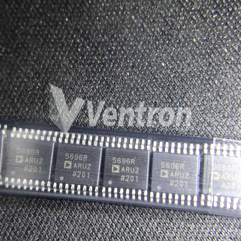
- IC DAC 16BIT MONO NON-LIN 28PLCC
- ECAD Model:
-
- Datasheet:
- AD569JP
Analog Devices Inc. AD569JP technical specifications, attributes, parameters and parts with similar specifications to Analog Devices Inc. AD569JP.
- Contact PlatingLead, Tin
- MountSurface Mount
- Mounting TypeSurface Mount
- Package / Case28-LCC (J-Lead)
- Number of Pins28
- Operating Temperature0°C~70°C
- PackagingTube
- JESD-609 Codee0
- Pbfree Codeno
- Part StatusObsolete
- Moisture Sensitivity Level (MSL)1 (Unlimited)
- Number of Terminations28
- ECCN CodeEAR99
- SubcategoryOther Converters
- Max Power Dissipation1W
- TechnologyBICMOS
- Terminal PositionQUAD
- Terminal FormJ BEND
- Peak Reflow Temperature (Cel)225
- Number of Functions1
- Supply Voltage12V
- Reflow Temperature-Max (s)30
- Base Part NumberAD569
- Pin Count28
- Output TypeVoltage - Buffered
- PolarityBipolar, Unipolar
- Max Supply Voltage13.2V
- Min Supply Voltage10.8V
- Nominal Supply Current9mA
- Number of Bits16
- ArchitectureSegmented DAC
- Converter TypeD/A CONVERTER
- Reference TypeExternal
- Data InterfaceParallel
- Differential OutputNo
- Resolution2 B
- Voltage - Supply, Analog±10.8V~13.2V
- Settling Time6μs
- Max Dual Supply Voltage13.2V
- Linearity Error-Max (EL)0.04%
- Min Dual Supply Voltage10.8V
- Input Bit CodeBINARY
- Dual Supply Voltage12V
- Number of Converters1
- INL/DNL (LSB)±0.02, ±0.5
- Negative Supply Voltage-Nom-12V
- Analog Output Voltage-Max5V
- Analog Output Voltage-Min-5V
- Height Seated (Max)4.57mm
- RoHS StatusNon-RoHS Compliant
- Lead FreeContains Lead
AD569JP Overview
Contact plating is an important aspect to consider when selecting electronic components. In this case, the contact plating for this particular device is lead and tin, which ensures a reliable and durable connection. The maximum supply voltage for this device is 13.2V, providing a wide range of power options. The nominal supply current is 9mA, ensuring efficient use of power. The reference type for this device is external, allowing for precise measurements and control. The data interface is parallel, allowing for fast and accurate data transfer. The minimum dual supply voltage is 10.8V, providing a stable power source. This device has 1 converter and the negative supply voltage-nom is -12V. The analog output voltage-min is -5V, providing a wide range of output options. It is important to note that this device is non-RoHS compliant, meaning it does not meet the standards for environmentally friendly materials.
AD569JP Features
28-LCC (J-Lead) package
28 pin count
28 pins
AD569JP Applications
There are a lot of Analog Devices Inc. AD569JP Digital to Analog Converters (DAC)?applications.
Wireless infrastructure:
Industrial Control Systems
Synchro Applications
Industrial Process Control
Microprocessor Controlled Circuits
Automatic Test Equipment
Motor Control
Process control equipment
Digital Audio Amplifiers
Synthesizers and Keyboards
AD569JP More Descriptions
DAC 1-CH Resistor-String 16-bit 28-Pin PLCC Tube
Digital to Analog Converters - DAC IC MONO 16-BIT
D/A Converter, 1 Func, Parallel, Word Input Loading, 4us Settling Time, PQCC28
28-LCC (J-Lead) Voltage - Buffered Segmented DAC S-PQCC-J28 digital to analog converter 5V 6mus 4.57mm 0C~70C
IC DAC 16BIT MONO NON-LIN 28PLCC
The AD569 is a monolithic 16-bit digital-to-analog converter (DAC) manufactured in Analog Devices' BiMOS II process. BiMOS II allows the fabrication of low power CMOS logic functions on the same chip as high precision bipolar linear circuitry. The AD569 chip includes two resistor strings, selector switches decoding logic, buffer amplifiers, and double-buffered input latches. The AD569's voltage-segmented architecture insures 16-bit monotonicity over time and temperature. Integral nonlinearity is maintained at ±0.01%, while differential nonlinearity is ±0.0004%. The on-chip, high-speed buffer amplifiers provide a voltage output settling time of 3 µs to within ±0.001% for a full-scale step. The reference input voltage which determines the output range can be either unipolar or bipolar. Nominal reference range is ±5 V and separate reference force and sense connections are provided for high accuracy applications. The AD569 can operate with an ac reference in multiplying applications. Data may be loaded into the AD569's input latches from 8- and 16-bit buses. The double-buffered structure simplifies 8-bit bus interfacing and allows multiple DACs to be loaded asynchronously and updated simultaneously. Four TTL/LSTTL/5 V CMOS-compatible signals control the latches: CS, LBE, HBE, and LDAC. The AD569 is available in five grades: J and K versions are specified from 0°C to 70°C and are packaged in a 28-pin plastic DIP and 28-pin PLCC package; AD and BD versions are specified from -25°C to 85°C and are packaged in a 28-pin ceramic DIP. The SD version, also in a 28-pin ceramic DIP, is specified from -55°C to 125°C.
The three parts on the right have similar specifications to AD569JP.
-
ImagePart NumberManufacturerContact PlatingMountMounting TypePackage / CaseNumber of PinsOperating TemperaturePackagingJESD-609 CodePbfree CodePart StatusMoisture Sensitivity Level (MSL)Number of TerminationsECCN CodeSubcategoryMax Power DissipationTechnologyTerminal PositionTerminal FormPeak Reflow Temperature (Cel)Number of FunctionsSupply VoltageReflow Temperature-Max (s)Base Part NumberPin CountOutput TypePolarityMax Supply VoltageMin Supply VoltageNominal Supply CurrentNumber of BitsArchitectureConverter TypeReference TypeData InterfaceDifferential OutputResolutionVoltage - Supply, AnalogSettling TimeMax Dual Supply VoltageLinearity Error-Max (EL)Min Dual Supply VoltageInput Bit CodeDual Supply VoltageNumber of ConvertersINL/DNL (LSB)Negative Supply Voltage-NomAnalog Output Voltage-MaxAnalog Output Voltage-MinHeight Seated (Max)RoHS StatusLead FreeFactory Lead TimeLifecycle StatusSurface MountSeriesPower SuppliesInterfacePower DissipationMax Output VoltageMin Input VoltageSlew RateMax Input VoltageSupply TypeSampling RateMin Output VoltageVoltage - Supply, DigitalIntegral Nonlinearity (INL)Conversion RateLengthDifferential NonlinearityNumber of DAC ChannelsHeightWidthREACH SVHCNumber of D/A ConvertersView Compare
-
 AD569JPLead, TinSurface MountSurface Mount28-LCC (J-Lead)280°C~70°CTubee0noObsolete1 (Unlimited)28EAR99Other Converters1WBICMOSQUADJ BEND225112V30AD56928Voltage - BufferedBipolar, Unipolar13.2V10.8V9mA16Segmented DACD/A CONVERTERExternalParallelNo2 B±10.8V~13.2V6μs13.2V0.04%10.8VBINARY12V1±0.02, ±0.5-12V5V-5V4.57mmNon-RoHS CompliantContains Lead-------------------------
 -
Gold-Surface Mount6-TSSOP, SC-88, SOT-3636-40°C~125°CTape & Reel (TR)e4noActive1 (Unlimited)6EAR99Other Converters500μWCMOSDUALGULL WING26013V40AD56126Voltage - BufferedUnipolar5.5V2.7V-10String DACD/A CONVERTERSupplyI2CNo1.25 B2.7V~5.5V10μs---BINARY-1±4 (Max), ±1 (Max)----ROHS3 CompliantContains Lead14 WeeksPRODUCTION (Last Updated: 1 month ago)YESnanoDAC®3/5V2-Wire, I2C, Serial550μW5.5V2.7V0.5 V/μs5.5VSingle1.7 Msps2.7V2.7V~5.5V4 LSB1.7 Msps2mm------
-
Tin-Surface Mount6-WDFN Exposed Pad, CSP6-40°C~125°CTape & Reel (TR)e3noActive1 (Unlimited)6EAR99Other Converters550μWCMOSDUAL-26013V30AD56016Voltage - BufferedBipolar, Unipolar5.5V2.7V75μA8String DACD/A CONVERTERSupplySPI, DSPNo1 B2.7V~5.5V10μs---BINARY--±0.5 (Max), ±0.5 (Max)----ROHS3 CompliantContains Lead20 WeeksPRODUCTION (Last Updated: 2 weeks ago)YESnanoDAC®3/5VSPI, Serial550μW5.5V2.7V0.5 V/μs5.5VSingle1.7 Msps2.7V2.7V~5.5V0.5 LSB1.7 Msps2.1mm0.5 LSB1750μm3.1mmNo SVHC-
-
--Surface MountDie00°C~70°CTray-noObsolete1 (Unlimited)16EAR99Other Converters-BIPOLARUPPER--15V-AD5610Current - Unbuffered----10R-2RD/A CONVERTERInternalParallelNo-4.5V~16.5V -10.8V~16.5V250ns---BINARY--±0.25, ±0.5-15V---Non-RoHS CompliantContains Lead--YES-----------4.5V~16.5V--------1
Popular Search Part Number
Related Keywords
Search Tags
Latest News
-
29 February 2024
4N35 Optocoupler: Pinout, Package, Application, and 4N25 vs 4N35
Ⅰ. Description of 4N35Ⅱ. 4N35 pinout and functionsⅢ. 4N35 technical parametersⅣ. How to use 4N35 optocoupler?Ⅴ. Application of 4N35 motorⅥ. How to test the 4N35 optocoupler?Ⅶ. 4N35 packageⅧ.... -
29 February 2024
TPS3808G01DBVR: A Powerful Power Monitoring Reset Chip
Ⅰ. What is TPS3808G01DBVR?Ⅱ. Functions of the TPS3808G01DBVRⅢ. TPS3808G01DBVR functional block diagramⅣ. Specifications of TPS3808G01DBVRⅤ. TPS3808G01DBVR shift register application in realityⅥ. Application circuit diagram of TPS3808G01DBVRⅦ. How to... -
01 March 2024
TPS92662AQPHPRQ1 Alternatives, Characteristics, Functions and Other Details
Ⅰ. Introduction to TPS92662AQPHPRQ1Ⅱ. Characteristics of TPS92662AQPHPRQ1Ⅲ. Functions of TPS92662AQPHPRQ1Ⅳ. Circuit diagram of the TPS92662AQPHPRQ1Ⅴ. How reliable is the TPS92662AQPHPRQ1?Ⅵ. TPS92662AQPHPRQ1 technical parametersⅦ. How does TPS92662AQPHPRQ1 perform fault... -
01 March 2024
BCM89811B1AWMLG Manufacturer, Characteristics, Specifications and Purchase Guide
Ⅰ. Overview of BCM89811B1AWMLGⅡ. Manufacturer of BCM89811B1AWMLGⅢ. What are the characteristics of BCM89811B1AWMLG?Ⅳ. Where is BCM89811B1AWMLG used?Ⅴ. What is the connection method of BCM89811B1AWMLG?Ⅵ. Specifications of BCM89811B1AWMLGⅦ. Competitive...
Help you to save your cost and time.
Reliable package for your goods.
Fast Reliable Delivery to save time.
Quality premium after-sale service.