.jpg)
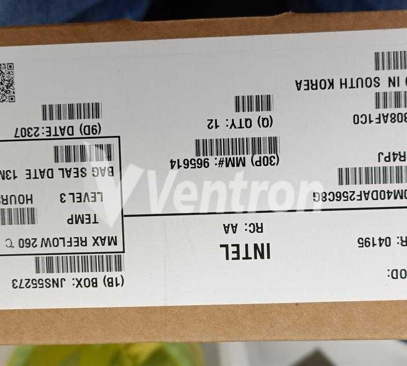
Altera 10M40DAF256I6G
- Part Number:
- 10M40DAF256I6G
- Manufacturer:
- Altera
- Ventron No:
- 3822652-10M40DAF256I6G
- Description:
- IC FPGA 178 I/O 256FBGA
- ECAD Model:
-


Altera 10M40DAF256I6G technical specifications, attributes, parameters and parts with similar specifications to Altera 10M40DAF256I6G.
- Mounting TypeSurface Mount
- Package / Case256-LBGA
- Surface MountYES
- Operating Temperature-40°C~100°C TJ
- PackagingTray
- SeriesMAX® 10
- JESD-609 Codee1
- Part StatusActive
- Moisture Sensitivity Level (MSL)3 (168 Hours)
- Number of Terminations256
- Terminal FinishTIN SILVER COPPER
- HTS Code8542.39.00.01
- Voltage - Supply1.15V~1.25V
- Terminal PositionBOTTOM
- Terminal FormBALL
- Peak Reflow Temperature (Cel)NOT SPECIFIED
- Time@Peak Reflow Temperature-Max (s)NOT SPECIFIED
- JESD-30 CodeS-PBGA-B256
- Number of I/O178
- Programmable Logic TypeFIELD PROGRAMMABLE GATE ARRAY
- Number of Logic Elements/Cells40000
- Total RAM Bits1290240
- Number of LABs/CLBs2500
- RoHS StatusRoHS Compliant
10M40DAF256I6G Overview
As part of the 256-LBGA package, it is included. This kind of FPGA is composed of FIELD PROGRAMMABLE GATE ARRAY. A total of 178 I/Os allow data to be transferred in a more coherent manner. A fundamental building block consists of 40000 logic elements/cells. With a Surface Mount connector, this FPGA module can be attached to the development board. In order to operate it, it requires a voltage supply of 1.15V~1.25V . It is a type of FPGA that belongs to the MAX® 10 series of FPGAs. Fpga chips is important to maintain the operating temperature wFpga chipshin the range of -40°C~100°C TJ when operating the machine. In order to save space, this FPGA model has been contained in Tray. There are a total of 256 terminations. This device has 1290240 RAM bits, which is the number of RAM bits that this device offers. The FPGA consists of 2500 LABs/CLBs.
10M40DAF256I6G Features
178 I/Os
Up to 1290240 RAM bits
10M40DAF256I6G Applications
There are a lot of Intel
10M40DAF256I6G FPGAs applications.
Bioinformatics
Device controllers
Software-defined radio
Random logic
ASIC prototyping
Medical imaging
Computer hardware emulation
Integrating multiple SPLDs
Voice recognition
Cryptography
10M40DAF256I6G More Descriptions
FPGA MAX 10 Family 40000 Cells Technology
IC FPGA 178 I/O 256FBGA MAX 10
IC FPGA 178 I/O 256FBGA MAX 10
The three parts on the right have similar specifications to 10M40DAF256I6G.
-
ImagePart NumberManufacturerMounting TypePackage / CaseSurface MountOperating TemperaturePackagingSeriesJESD-609 CodePart StatusMoisture Sensitivity Level (MSL)Number of TerminationsTerminal FinishHTS CodeVoltage - SupplyTerminal PositionTerminal FormPeak Reflow Temperature (Cel)Time@Peak Reflow Temperature-Max (s)JESD-30 CodeNumber of I/OProgrammable Logic TypeNumber of Logic Elements/CellsTotal RAM BitsNumber of LABs/CLBsRoHS StatusFactory Lead TimeSubcategoryTechnologySupply VoltageTerminal PitchReflow Temperature-Max (s)Number of OutputsQualification StatusPower SuppliesNumber of InputsView Compare
-
 10M40DAF256I6GSurface Mount256-LBGAYES-40°C~100°C TJTrayMAX® 10e1Active3 (168 Hours)256TIN SILVER COPPER8542.39.00.011.15V~1.25VBOTTOMBALLNOT SPECIFIEDNOT SPECIFIEDS-PBGA-B256178FIELD PROGRAMMABLE GATE ARRAY4000012902402500RoHS Compliant-----------
 -
Surface Mount484-BGAYES-40°C~100°C TJTrayMAX® 10e1Active3 (168 Hours)484TIN SILVER COPPER-1.15V~1.25VBOTTOMBALLNOT SPECIFIEDNOT SPECIFIEDS-PBGA-B484360FIELD PROGRAMMABLE GATE ARRAY4000012902402500RoHS Compliant----------
-
Surface Mount484-BGAYES-40°C~100°C TJTrayMAX® 10e1Active3 (168 Hours)484Tin/Silver/Copper (Sn/Ag/Cu)8542.39.00.011.15V~1.25VBOTTOMBALLNOT SPECIFIED-S-PBGA-B484360FIELD PROGRAMMABLE GATE ARRAY4000012902402500RoHS Compliant8 WeeksField Programmable Gate ArraysCMOS1.2V1mmNOT SPECIFIED360Not Qualified1.2V360
-
Surface Mount672-BGAYES0°C~85°C TJTrayMAX® 10e1Active3 (168 Hours)672Tin/Silver/Copper (Sn/Ag/Cu)-1.15V~1.25VBOTTOMBALLNOT SPECIFIED-S-PBGA-B672500FIELD PROGRAMMABLE GATE ARRAY4000012902402500RoHS Compliant8 WeeksField Programmable Gate ArraysCMOS1.2V1mmNOT SPECIFIED500Not Qualified1.2V500
Popular Search Part Number
Related Keywords
Search Tags
Latest News
-
28 December 2023
74HC573 Transparent Latch Functions, Working Principle, Usage and Application
Ⅰ. What is a latch?Ⅱ. Overview of 74HC573Ⅲ. Pin configuration of 74HC573 latchⅣ. Functions of 74HC573 latchⅤ. How does 74HC573 latch work?Ⅵ. How to use 74HC573 latch?Ⅶ. Practical... -
29 December 2023
An Introduction to HEF4093BP CMOS NAND Schmitt Trigger
Ⅰ. What is HEF4093BP?Ⅱ. Symbol, footprint and 3D model of HEF4093BPⅢ. The specifications of HEF4093BPⅣ. Limiting values of HEF4093BPⅤ. How does HEF4093BP work?Ⅵ. HEF4093BP's market trendⅦ. Where is... -
29 December 2023
TPS54331DR Converter Replacements, Characteristics, Applications and Other Details
Ⅰ. Overview of TPS54331DRⅡ. Characteristics of TPS54331DR converterⅢ. Technical parameters of TPS54331DRⅣ. Typical application of TPS54331DR converterⅤ. Programming the slow start time of TPS54331DRⅥ. Pin configuration of TPS54331DR... -
02 January 2024
STM32F030C8T6 Microcontroller Features, Specifications, Package, Usage and Applications
Ⅰ. What is STM32F030C8T6?Ⅱ. What are the features of STM32F030C8T6?Ⅲ. Specifications of STM32F030C8T6Ⅳ. STM32F030C8T6 Flash reading and writingⅤ. Package of STM32F030C8T6Ⅵ. How to use STM32F030C8T6?Ⅶ. Where is STM32F030C8T6...
Help you to save your cost and time.
Reliable package for your goods.
Fast Reliable Delivery to save time.
Quality premium after-sale service.