
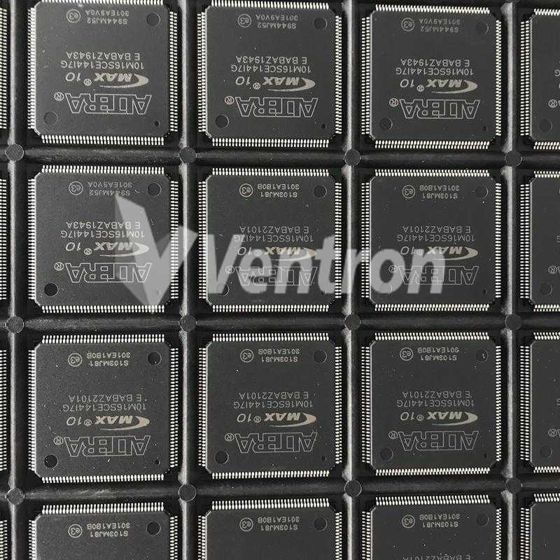
Altera 10M16SCE144I7G
- Part Number:
- 10M16SCE144I7G
- Manufacturer:
- Altera
- Ventron No:
- 3632310-10M16SCE144I7G
- Description:
- IC FPGA 101 I/O 144EQFP
- ECAD Model:
-
Altera 10M16SCE144I7G technical specifications, attributes, parameters and parts with similar specifications to Altera 10M16SCE144I7G.
- Factory Lead Time11 Weeks
- Mounting TypeSurface Mount
- Package / Case144-LQFP Exposed Pad
- Surface MountYES
- Operating Temperature-40°C~100°C TJ
- PackagingTray
- SeriesMAX® 10
- Part StatusActive
- Moisture Sensitivity Level (MSL)3 (168 Hours)
- Number of Terminations144
- HTS Code8542.39.00.01
- SubcategoryField Programmable Gate Arrays
- TechnologyCMOS
- Voltage - Supply2.85V~3.465V
- Terminal PositionQUAD
- Terminal FormGULL WING
- Peak Reflow Temperature (Cel)NOT SPECIFIED
- Terminal Pitch0.5mm
- Reflow Temperature-Max (s)NOT SPECIFIED
- JESD-30 CodeS-PQFP-G144
- Number of Outputs101
- Qualification StatusNot Qualified
- Power Supplies3/3.3V
- Number of I/O101
- Number of Inputs101
- Programmable Logic TypeFIELD PROGRAMMABLE GATE ARRAY
- Number of Logic Elements/Cells16000
- Total RAM Bits562176
- Number of LABs/CLBs1000
- RoHS StatusRoHS Compliant
10M16SCE144I7G Overview
This component is manufactured by Altera and falls under the Embedded - FPGAs category. Specifically, it is an Embedded - FPGAs (Field Programmable Gate Array) chip. It is designed to be mounted on a surface and comes packaged in a tray. The part is currently in active production. It utilizes CMOS technology and requires a voltage supply between 2.85V and 3.465V. The terminal position is QUAD, meaning it has four terminals. The maximum reflow temperature for this chip is not specified. It contains 16000 logic elements/cells and has a total of 562176 bits of RAM. This component is also RoHS compliant, meaning it meets the standards for Restriction of Hazardous Substances.
10M16SCE144I7G Features
101 I/Os
Up to 562176 RAM bits
10M16SCE144I7G Applications
There are a lot of Intel 10M16SCE144I7G FPGAs applications.
Medical Applications
Broadcast
Digital signal processing
Scientific Instruments
Integrating multiple SPLDs
Medical imaging
Enterprise networking
Automotive driver's assistance
Software-defined radio
Wireless Communications
10M16SCE144I7G More Descriptions
FPGA - Field Programmable Gate Array non-volatile FPGA, 101 I/O, 144EQFP
FPGA MAX 10 Family 16000 Cells 55nm Technology 3.3V 144-Pin EQFP EP
Field Programmable Gate Array, 16000-Cell, CMOS, PQFP144
CMOS 2016 RoHS Compliant GULL WING FPGA 100C 68.6kB 3.465V 0.5mm
IC FPGA/CPLD NV 101 I/O 144EQFP
FPGA MAX 10 Family 16000 Cells 55nm Technology 3.3V 144-Pin EQFP EP
Field Programmable Gate Array, 16000-Cell, CMOS, PQFP144
CMOS 2016 RoHS Compliant GULL WING FPGA 100C 68.6kB 3.465V 0.5mm
IC FPGA/CPLD NV 101 I/O 144EQFP
The three parts on the right have similar specifications to 10M16SCE144I7G.
-
ImagePart NumberManufacturerFactory Lead TimeMounting TypePackage / CaseSurface MountOperating TemperaturePackagingSeriesPart StatusMoisture Sensitivity Level (MSL)Number of TerminationsHTS CodeSubcategoryTechnologyVoltage - SupplyTerminal PositionTerminal FormPeak Reflow Temperature (Cel)Terminal PitchReflow Temperature-Max (s)JESD-30 CodeNumber of OutputsQualification StatusPower SuppliesNumber of I/ONumber of InputsProgrammable Logic TypeNumber of Logic Elements/CellsTotal RAM BitsNumber of LABs/CLBsRoHS StatusJESD-609 CodeTerminal FinishTime@Peak Reflow Temperature-Max (s)Supply VoltageView Compare
-
 10M16SCE144I7G11 WeeksSurface Mount144-LQFP Exposed PadYES-40°C~100°C TJTrayMAX® 10Active3 (168 Hours)1448542.39.00.01Field Programmable Gate ArraysCMOS2.85V~3.465VQUADGULL WINGNOT SPECIFIED0.5mmNOT SPECIFIEDS-PQFP-G144101Not Qualified3/3.3V101101FIELD PROGRAMMABLE GATE ARRAY160005621761000RoHS Compliant-----
 -
-Surface Mount484-BGAYES-40°C~100°C TJTrayMAX® 10Active3 (168 Hours)484---1.15V~1.25VBOTTOMBALLNOT SPECIFIED--S-PBGA-B484---320-FIELD PROGRAMMABLE GATE ARRAY160005621761000RoHS Compliante1TIN SILVER COPPERNOT SPECIFIED-
-
-Surface Mount256-LBGAYES-40°C~100°C TJTrayMAX® 10Active3 (168 Hours)256---1.15V~1.25VBOTTOMBALLNOT SPECIFIED--S-PBGA-B256---178-FIELD PROGRAMMABLE GATE ARRAY160005621761000RoHS Compliante1TIN SILVER COPPERNOT SPECIFIED-
-
-Surface Mount256-LBGAYES-40°C~125°C TJTrayMAX® 10Active3 (168 Hours)2568542.39.00.01Field Programmable Gate ArraysCMOS1.15V~1.25VBOTTOMBALLNOT SPECIFIED1mmNOT SPECIFIEDS-PBGA-B256178Not Qualified1.2V178178FIELD PROGRAMMABLE GATE ARRAY160005621761000RoHS Compliante1Tin/Silver/Copper (Sn/Ag/Cu)-1.2V

Popular Search Part Number
Related Keywords
Search Tags
Latest News
-
25 September 2023
A Comparison of 2N7000 and BS170 N-Channel Mosfet Transistors
Ⅰ. What is a MOS field effect transistor?Ⅱ. Overview of 2N7000Ⅲ. Overview of BS170Ⅳ. 2N7000 vs BS170: PCB footprintsⅤ. 2N7000 vs BS170: Technical parametersⅥ. 2N7000 vs BS170: FeaturesⅦ.... -
26 September 2023
W25Q128JVSIQ Footprint, Features and Package
Ⅰ. W25Q128JVSIQ descriptionⅡ. W25Q128JVSIQ symbol and footprintⅢ. Technical parametersⅣ. Features of W25Q128JVSIQⅤ. Pin configuration of W25Q128JVSIQⅥ. Package of W25Q128JVSIQⅦ. What are the characteristics of the SPI interface of... -
26 September 2023
TDA7560 Audio Power Amplifier: Symbol, Features and Application
Ⅰ. Overview of TDA7560Ⅱ. Pin connection, symbol and footprint of TDA7560Ⅲ. Technical parametersⅣ. Features of TDA7560Ⅴ. Application of TDA7560Ⅵ. Are TDA7560 and TDA7851 interchangeable?Ⅶ. TDA7560 car power amplifier... -
27 September 2023
BC640 PNP Transistor: Features, Package and Other Details
Ⅰ. Overview of BC640Ⅱ. Symbol and footprint of BC640Ⅲ. Technical parametersⅣ. Features of BC640Ⅴ. Pinout and package of BC640Ⅵ. Application of BC640Ⅶ. How to optimize the performance of...
Help you to save your cost and time.
Reliable package for your goods.
Fast Reliable Delivery to save time.
Quality premium after-sale service.