
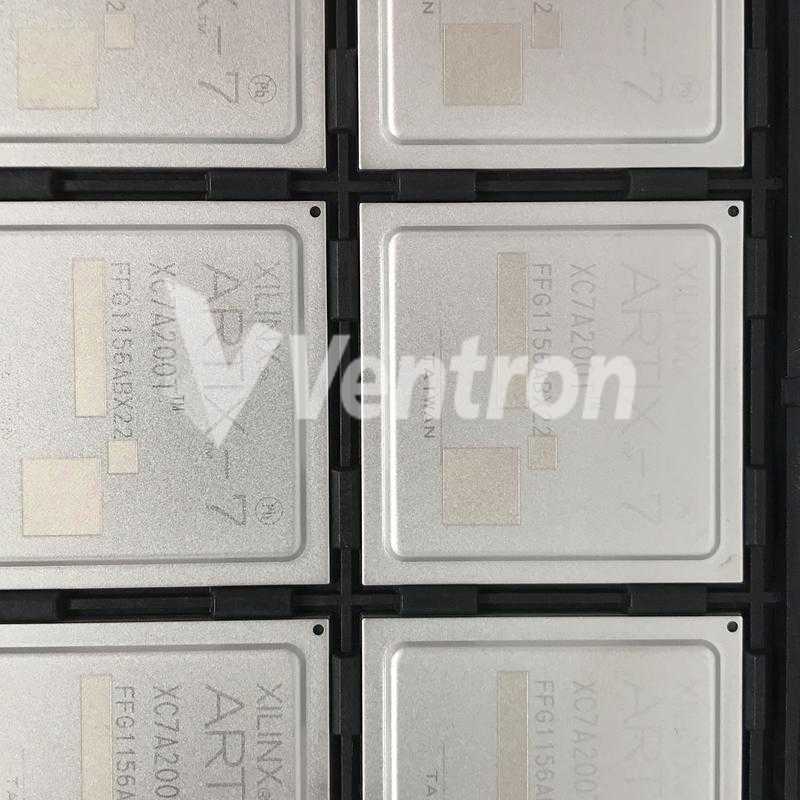
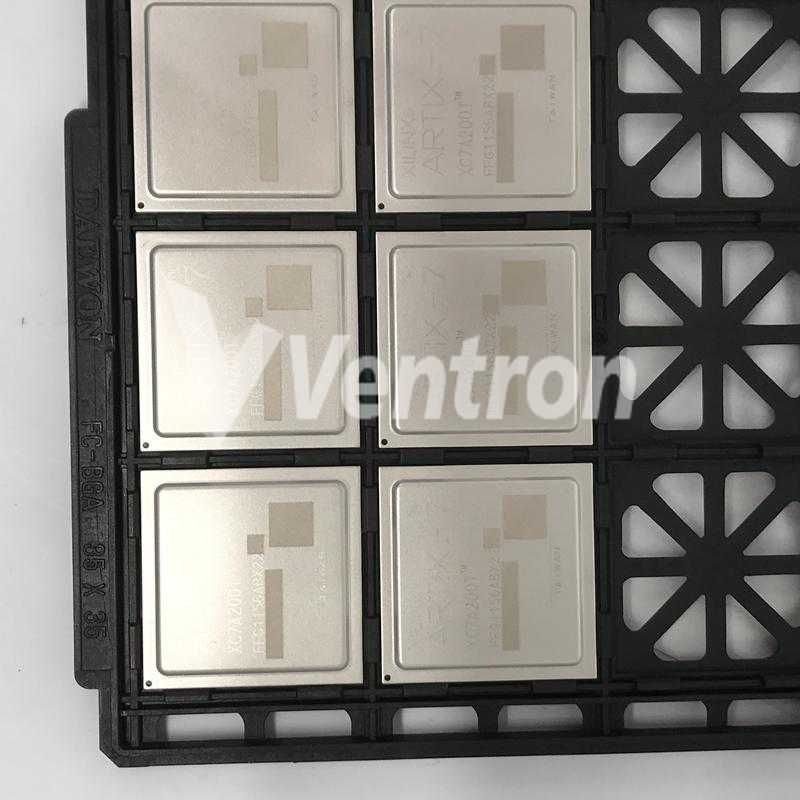
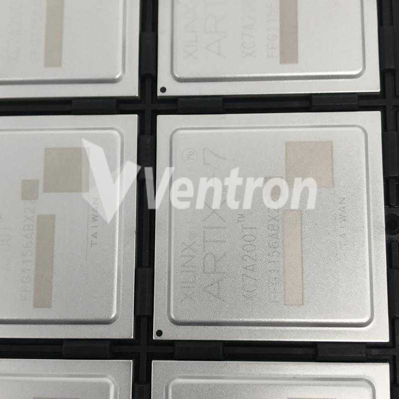
Xilinx Inc. XC7A200T-2FFG1156I
- Part Number:
- XC7A200T-2FFG1156I
- Manufacturer:
- Xilinx Inc.
- Ventron No:
- 3821611-XC7A200T-2FFG1156I
- Description:
- IC FPGA ARTIX7 500 I/O 1156FCBGA
- ECAD Model:
-
- Datasheet:
- XC7A200T-2FFG1156I


Xilinx Inc. XC7A200T-2FFG1156I technical specifications, attributes, parameters and parts with similar specifications to Xilinx Inc. XC7A200T-2FFG1156I.
- Factory Lead Time10 Weeks
- Contact PlatingCopper, Silver, Tin
- Mounting TypeSurface Mount
- Package / Case1156-BBGA, FCBGA
- Surface MountYES
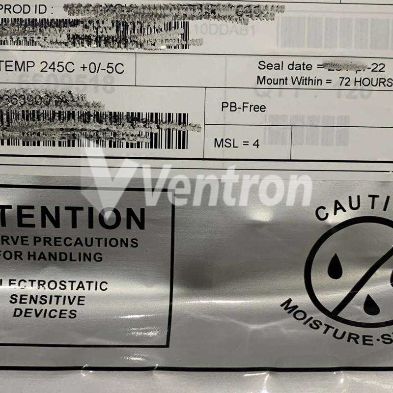
- Operating Temperature-40°C~100°C TJ
- PackagingTray
- Published2009
- SeriesArtix-7
- JESD-609 Codee1
- Pbfree Codeyes
- Part StatusActive
- Moisture Sensitivity Level (MSL)4 (72 Hours)
- ECCN Code3A991.D
- Terminal FinishTin/Silver/Copper (Sn96.5Ag3.0Cu0.5)
- HTS Code8542.39.00.01
- SubcategoryField Programmable Gate Arrays
- TechnologyCMOS
- Voltage - Supply0.95V~1.05V
- Terminal PositionBOTTOM
- Terminal FormBALL
- Supply Voltage1V
- Terminal Pitch1mm
- Base Part NumberXC7A200T
- JESD-30 CodeS-PBGA-B1156
- Number of Outputs500
- Power Supplies1V
- Memory Size1GB
- Number of I/O500
- RAM Size1.6MB
- Memory TypeDDR3
- Clock Frequency1286MHz
- Propagation Delay110 ps
- Turn On Delay Time110 ps
- Number of Inputs500
- Programmable Logic TypeFIELD PROGRAMMABLE GATE ARRAY
- Number of Logic Elements/Cells215360
- Total RAM Bits13455360
- Number of LABs/CLBs16825
- Speed Grade-2
- Number of Registers269200
- Combinatorial Delay of a CLB-Max1.05 ns
- Height Seated (Max)3.1mm
- Length35mm
- Width35mm
- Radiation HardeningNo
- RoHS StatusROHS3 Compliant
XC7A200T-2FFG1156I Overview
This package is included in the 1156-BBGA, FCBGA package and is available for purchase. Fpga chips consists of FIELD PROGRAMMABLE GATE ARRAY elements. The I/Os are designed to facilitate a more coherent transfer of data. Logic elements/cells form the fundamental building block of a computer. Power is provided by a 1V-volt supply. The Field Programmable Gate Arrays family of FPGA parts includes this part. By attaching the Surface Mount connector, you can use this FPGA module with your development board. A supply voltage of 0.95V~1.05V is needed in order for fpga chips to operate. The Artix-7 Series is one of the types of FPGAs that belong to this type. In order to ensure a safe and efficient operation, it is important to maintain a temperature within -40°C~100°C TJ at all times. A device such as this one has 500 outputs built into it. Unlike other FPGA models, this one is contained in Tray for the sake of space saving. Fpga chips is important to note that this device has a RAM capacFpga chipsy of 13455360 bFpga chipss. Parts related to this part can be found using its base part number XC7A200T. Fpga electronics is important that this FPGA module has a RAM si1.6MBe of 1.6MB in order to ensure that the program will run normally. Fpga electronics contains 16825 LABs/CLBs in an array. Powered by a 1V power supply, it can be operated by almost anyone. Typically, it uses a crystal oscillating at 1286MHz in order to operate. Programs and data can be stored in the 1GB memory embedded in this FPGA module. Fpga semiconductor is important to note that the data is stored and transferred in 269200 different registers. The DDR3 memory is adopted for storing data and avoiding resource conflicts.
XC7A200T-2FFG1156I Features
500 I/Os
Up to 13455360 RAM bits
269200 registers
XC7A200T-2FFG1156I Applications
There are a lot of Xilinx Inc. XC7A200T-2FFG1156I FPGAs applications.
Filtering and communication encoding
Data Mining
Medical Electronics
Computer hardware emulation
Consumer Electronics
Military DSP
Distributed Monetary Systems
Defense Applications
Video & Image Processing
Security systems
XC7A200T-2FFG1156I More Descriptions
Field Programmable Gate Array, 16825 CLBs, 1286MHz, 215360-Cell, PBGA1156
Artix-7 XC7A200T 1156-BBGA FCBGA Tin/Silver/Copper (Sn96.5Ag3.0Cu0.5) field programmable gate array 3.1mm 1V 1286MHz 110ps
FPGA, ARTIX-7, 500 I/O, FCBGA-1156; No. of Logic Blocks:33650; No. of Macrocells:215360Macrocells; FPGA Family:Artix-7; Logic Case Style:FCBGA; No. of Pins:1156Pins; No. of Speed Grades:2; Total RAM Bits:13140Kbit; MSL:- RoHS Compliant: Yes
The three parts on the right have similar specifications to XC7A200T-2FFG1156I.
-
ImagePart NumberManufacturerFactory Lead TimeContact PlatingMounting TypePackage / CaseSurface MountOperating TemperaturePackagingPublishedSeriesJESD-609 CodePbfree CodePart StatusMoisture Sensitivity Level (MSL)ECCN CodeTerminal FinishHTS CodeSubcategoryTechnologyVoltage - SupplyTerminal PositionTerminal FormSupply VoltageTerminal PitchBase Part NumberJESD-30 CodeNumber of OutputsPower SuppliesMemory SizeNumber of I/ORAM SizeMemory TypeClock FrequencyPropagation DelayTurn On Delay TimeNumber of InputsProgrammable Logic TypeNumber of Logic Elements/CellsTotal RAM BitsNumber of LABs/CLBsSpeed GradeNumber of RegistersCombinatorial Delay of a CLB-MaxHeight Seated (Max)LengthWidthRadiation HardeningRoHS StatusMountNumber of PinsNumber of TerminationsMax Operating TemperatureMin Operating TemperatureAdditional FeaturePeak Reflow Temperature (Cel)Time@Peak Reflow Temperature-Max (s)Supply Voltage-Max (Vsup)Supply Voltage-Min (Vsup)Number of Logic Blocks (LABs)Reflow Temperature-Max (s)Pin CountQualification StatusOperating Supply VoltageView Compare
-
 XC7A200T-2FFG1156I10 WeeksCopper, Silver, TinSurface Mount1156-BBGA, FCBGAYES-40°C~100°C TJTray2009Artix-7e1yesActive4 (72 Hours)3A991.DTin/Silver/Copper (Sn96.5Ag3.0Cu0.5)8542.39.00.01Field Programmable Gate ArraysCMOS0.95V~1.05VBOTTOMBALL1V1mmXC7A200TS-PBGA-B11565001V1GB5001.6MBDDR31286MHz110 ps110 ps500FIELD PROGRAMMABLE GATE ARRAY2153601345536016825-22692001.05 ns3.1mm35mm35mmNoROHS3 Compliant----------------
 -
---------e1---EAR99Tin/Silver/Copper (Sn/Ag/Cu)8542.39.00.01---BOTTOMBALL0.9V1mm-----170112.5kB-----FIELD PROGRAMMABLE GATE ARRAY16640----1.51 ns1.55mm17mm17mm-RoHS CompliantSurface Mount256256100°C0°CALSO OPERATES AT 1V SUPPLYNOT SPECIFIEDNOT SPECIFIED0.93V0.87V1300----
-
10 WeeksCopper, Silver, TinSurface Mount256-LBGA-0°C~85°C TJTray2010Artix-7e1yesActive3 (168 Hours)EAR99Tin/Silver/Copper (Sn/Ag/Cu)-Field Programmable Gate ArraysCMOS0.95V~1.05VBOTTOMBALL1V---1701V-170337.5kB--1.09 ns1.09 ns-FIELD PROGRAMMABLE GATE ARRAY5216027648004075165200-----ROHS3 CompliantSurface Mount256256---NOT SPECIFIED----NOT SPECIFIED256Not Qualified-
-
11 Weeks-Surface Mount484-BBGA, FCBGA--40°C~100°C TJTray2009Artix-7e0-Active4 (72 Hours)-TIN LEAD---0.95V~1.05VBOTTOMBALL1V-XC7A200TS-PBGA-B484---2851.6MB--130 ps--FIELD PROGRAMMABLE GATE ARRAY21536013455360168251269200-2.54mm23mm23mmNoNon-RoHS CompliantSurface Mount-484-----------1V
Popular Search Part Number
Related Keywords
Search Tags
Latest News
-
07 November 2023
TLP250 MOSFET IGBT Driver: Manufacturer, Footprint and Applications
Ⅰ. Overview of TLP250Ⅱ. Manufacturer of TLP250Ⅲ. TLP250 symbol, footprint and pin configurationⅣ. What are the features of TLP250?Ⅴ. Technical parameters of TLP250Ⅵ. How to use TLP250 isolated... -
07 November 2023
LM2596 Voltage Regulator: Equivalents, Features, Structure and Applications
Ⅰ. What is a voltage regulator?Ⅱ. Overview of LM2596 voltage regulatorⅢ. Features of LM2596 voltage regulatorⅣ. Pin configuration of LM2596 voltage regulatorⅤ. Structure of LM2596 voltage regulatorⅥ. LM2596... -
08 November 2023
What is MOC3021 Optocoupler Triac Driver?
Ⅰ. What is an optocoupler?Ⅱ. Overview of MOC3021 optocouplerⅢ. Pin configuration of MOC3021 optocouplerⅣ. Features of MOC3021 optocouplerⅤ. Technical parameters of MOC3021 optocouplerⅥ. Working principle of MOC3021 optocouplerⅦ.... -
08 November 2023
LM324 vs LM358: What is the Difference Between Them?
Ⅰ. What is an operational amplifier?Ⅱ. Overview of LM324Ⅲ. Overview of LM358Ⅳ. LM324 vs LM358: FeaturesⅤ. LM324 vs LM358: Technical parametersⅥ. LM324 vs LM358: Pin configurationⅦ. LM324 vs...
Help you to save your cost and time.
Reliable package for your goods.
Fast Reliable Delivery to save time.
Quality premium after-sale service.