
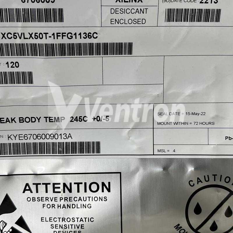
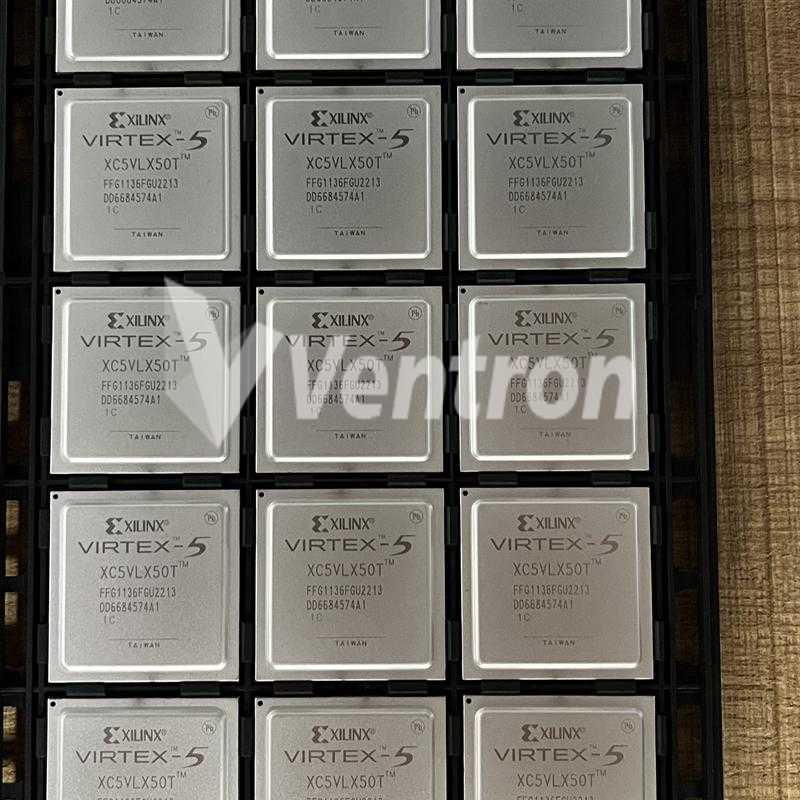
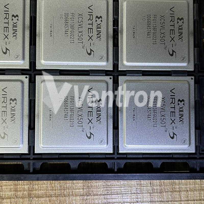
Xilinx Inc. XC5VLX50T-1FFG665C
- Part Number:
- XC5VLX50T-1FFG665C
- Manufacturer:
- Xilinx Inc.
- Ventron No:
- 3635144-XC5VLX50T-1FFG665C
- Description:
- IC FPGA 360 I/O 665FCBGA
- ECAD Model:
-
- Datasheet:
- XC5VLX50T-1FFG665C
Xilinx Inc. XC5VLX50T-1FFG665C technical specifications, attributes, parameters and parts with similar specifications to Xilinx Inc. XC5VLX50T-1FFG665C.
- Factory Lead Time10 Weeks
- MountSurface Mount
- Mounting TypeSurface Mount
- Package / Case665-BBGA, FCBGA
- Number of Pins665
- Operating Temperature0°C~85°C TJ
- PackagingTray
- Published1999
- SeriesVirtex®-5 LXT
- JESD-609 Codee1
- Pbfree Codeyes
- Part StatusActive
- Moisture Sensitivity Level (MSL)4 (72 Hours)
- Number of Terminations665
- Terminal FinishTin/Silver/Copper (Sn95.5Ag4.0Cu0.5)
- SubcategoryField Programmable Gate Arrays
- TechnologyCMOS
- Voltage - Supply0.95V~1.05V
- Terminal PositionBOTTOM
- Terminal FormBALL
- Peak Reflow Temperature (Cel)250
- Supply Voltage1V
- Reach Compliance Codenot_compliant
- Reflow Temperature-Max (s)30
- Base Part NumberXC5VLX50
- Pin Count665
- Number of Outputs360
- Qualification StatusNot Qualified
- Number of I/O360
- RAM Size270kB
- Programmable Logic TypeFIELD PROGRAMMABLE GATE ARRAY
- Number of Logic Elements/Cells46080
- Total RAM Bits2211840
- Number of LABs/CLBs3600
- Speed Grade1
- Number of Macro Cells330000
- Height2.4mm
- Length27mm
- Width27mm
- REACH SVHCUnknown
- RoHS StatusROHS3 Compliant
XC5VLX50T-1FFG665C Overview
The Mount is Surface Mount, which means it is designed to be mounted directly onto the surface of a circuit board. This type of mount is commonly used in electronic devices and offers a more compact and efficient design. The Moisture Sensitivity Level (MSL) for this component is 4, which indicates that it can withstand exposure to moisture for up to 72 hours without being damaged. The Terminal Form for this component is BALL, which refers to the shape of the terminal used for connecting the component to the circuit board. The Reach Compliance Code is not_compliant, which means it does not meet certain environmental regulations. The Reflow Temperature-Max (s) is 30, indicating the maximum temperature that this component can withstand during the reflow process. With a Pin Count of 665, this component offers a high level of connectivity. However, it is important to note that its Qualification Status is Not Qualified, meaning it has not yet undergone the necessary testing and certification. The Speed Grade of 1 indicates that this component has a high-speed performance. Its Height is 2.4mm and Length is 27mm, making it a compact and space-saving option for electronic devices.
XC5VLX50T-1FFG665C Features
360 I/Os
Up to 2211840 RAM bits
665 LABs/CLBs
XC5VLX50T-1FFG665C Applications
There are a lot of Xilinx Inc. XC5VLX50T-1FFG665C FPGAs applications.
Solar Energy
Automotive driver's assistance
Telecommunication
Medical imaging
Automation
ADAS
Broadcast
Camera time adjustments
Medical ultrasounds
Medical Electronics
XC5VLX50T-1FFG665C More Descriptions
FPGA Virtex-5 LXT Family 46080 Cells 65nm (CMOS) Technology 1V 665-Pin FCBGA
Field Programmable Gate Array, 3600 CLBs, 46080-Cell, PBGA665
FPGA - Field Programmable Gate Array XC5VLX50T-1FFG665C
FPGA, VIRTEX-5 LXT, 50K, 665FCBGA
Product Description Demo for Development.
French Electronic Distributor since 1988
XC5VLX50T-1FFG665C ROHS COMPLIANT: YES
FPGA, VIRTEX-5 LXT, 50K, 665FCBGA; No. of Logic Blocks:7200; Family Type:Virtex-5; No. of Speed Grades:1; Total RAM Bits:2211840; No. of I/O's:360; Clock Management:DCM, PLL; Core Supply Voltage Range:1V; I/O Supply Voltage:3.3V; Operating Frequency Max:550MHz; Operating Temperature Range:0°C to 85°C; Logic Case Style:BGA; No. of Pins:665; MSL:MSL 3 - 168 hours; SVHC:No SVHC (20-Jun-2011)
Popular Search Part Number
Related Keywords
Search Tags
Latest News
-
19 September 2023
Comparison Between 2N3055 vs TIP3055
Ⅰ. Overview of 2N3055Ⅱ. Overview of TIP3055Ⅲ. Pin diagram comparisonⅣ. Technical parametersⅤ. Comparison of current amplification factorsⅥ. Package comparisonⅦ. Symbol of 2N3055 and TIP3055Ⅷ. Application scenarios comparisonⅨ. Can... -
19 September 2023
STM32F303CCT6 Microcontroller: Footprint, Equivalent and Advantages
Ⅰ. What is STM32F303CCT6?Ⅱ. 3D Model and footprint of STM32F303CCT6Ⅲ. Technical parametersⅣ. Features of STM32F303CCT6Ⅴ. Package and packaging of STM32F303CCT6Ⅵ. Typical and maximum current consumptionⅦ. Advantages of STM32F303CCT6... -
20 September 2023
ATMEGA8-16PU Microcontroller: Symbol, Equivalent and Electrical Characteristics
Ⅰ. Overview of ATMEGA8-16PUⅡ. Symbol, Footprint and Pin Configuration of ATMEGA8-16PUⅢ. Technical parametersⅣ. Electrical characteristics of ATMEGA8-16PUⅤ. What is the difference between ATMEGA8-16PU and ATMEGA8-16PI?Ⅵ. I/O Memory of... -
20 September 2023
The Pinout, Advantages, and Electrical Characteristics of AO4466
Ⅰ. What is AO4466?Ⅱ. Symbol, Pinout and Footprint of AO4466Ⅲ. Technical parametersⅣ. What are the advantages of AO4466?Ⅴ. Application fields of AO4466Ⅵ. Typical electrical characteristicsⅦ. How to detect...

Help you to save your cost and time.
Reliable package for your goods.
Fast Reliable Delivery to save time.
Quality premium after-sale service.