
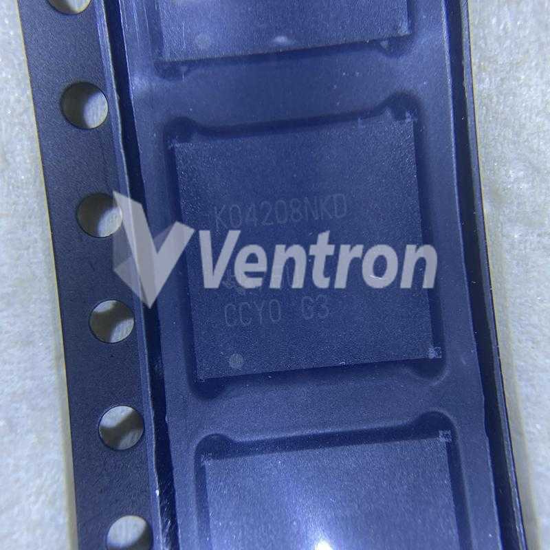
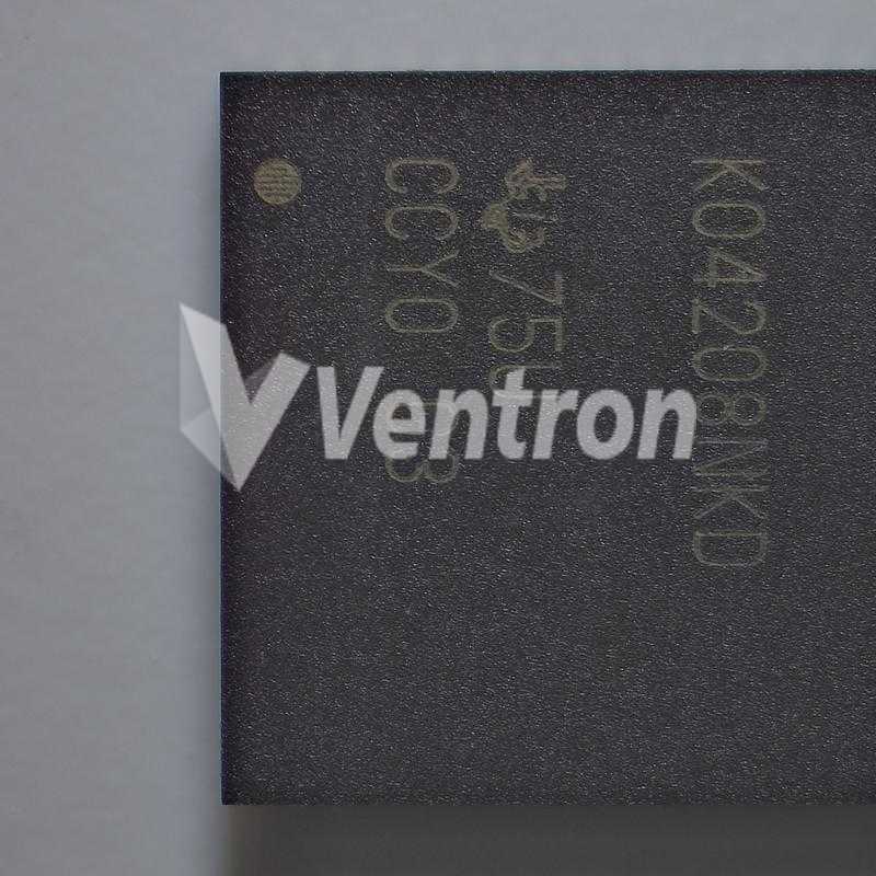
Texas Instruments LMK04208NKDR
- Part Number:
- LMK04208NKDR
- Manufacturer:
- Texas Instruments
- Ventron No:
- 2977657-LMK04208NKDR
- Description:
- IC CLOCK DUAL PLL 64WQFN
- ECAD Model:
-
- Datasheet:
- LMK04208NKDR
Description
The LMK04208 is a high-performance clock conditioner with superior clock jitter cleaning, generation, and distribution capabilities. It features a dual-loop PLLatinum™ architecture that enables ultra-low RMS jitter performance of 111 fs (12 kHz to 20 MHz) when paired with a low-noise VCXO module or sub-200 fs rms jitter (12 kHz to 20 MHz) with an external crystal and varactor diode.
The dual-loop architecture consists of two high-performance phase-locked loops (PLLs), a low-noise crystal oscillator circuit, and a high-performance voltage-controlled oscillator (VCO). PLL1 provides low-noise jitter cleaner functionality, while PLL2 performs clock generation. PLL1 can be configured to work with an external VCXO module or the integrated crystal oscillator with an external tunable crystal and varactor diode. When paired with a narrow loop bandwidth, PLL1 utilizes the superior close-in phase noise of the VCXO module or tunable crystal to clean the input clock. The output of PLL1 serves as the clean input reference for PLL2, which locks the integrated VCO. PLL2's loop bandwidth can be optimized to clean the far-out phase noise where the integrated VCO outperforms the VCXO module or tunable crystal used in PLL1.
Features
Ultra-low RMS jitter performance:
111 fs, RMS jitter (12 kHz to 20 MHz)
123 fs, RMS jitter (100 Hz to 20 MHz)
Dual-loop PLLatinum™ PLL architecture
Integrated low-noise crystal oscillator circuit
Holdover mode when input clocks are lost
Automatic or manual triggering/recovery
PLL2-normalized PLL noise floor of -227 dBc/Hz
Phase detector rate of up to 155 MHz
OSCin frequency-doubler
Integrated low-noise VCO or external VCO mode
Two redundant input clocks with LOS-automatic and manual switch-over modes
50% duty cycle output divides, 1 to 1045 (even and odd)
6 LVPECL, LVDS, or LVCMOS programmable outputs
Digital delay: fixed or dynamically adjustable 25 ps step
Analog delay control
7 differential outputs
Up to 14 single-ended outputs
Up to 6 VCXO/crystal buffered outputs
Clock rates of up to 1536 MHz
0-delay mode
Three default clock outputs at power up
Multi-mode: dual PLL, single PLL, and clock distribution
Industrial temperature range: -40°C to 85°C
3.15-V to 3.45-V operation
64-pin WQFN package (9.0 x 9.0 x 0.8 mm)
Applications
Clock distribution
Data converter clocking
Wireless infrastructure
Networking, SONET/SDH, DSLAM
Medical, video, military, aerospace
Test and measurement
Texas Instruments LMK04208NKDR technical specifications, attributes, parameters and parts with similar specifications to Texas Instruments LMK04208NKDR.
- Factory Lead Time6 Weeks
- Lifecycle StatusACTIVE (Last Updated: 5 days ago)
- MountSurface Mount
- Mounting TypeSurface Mount
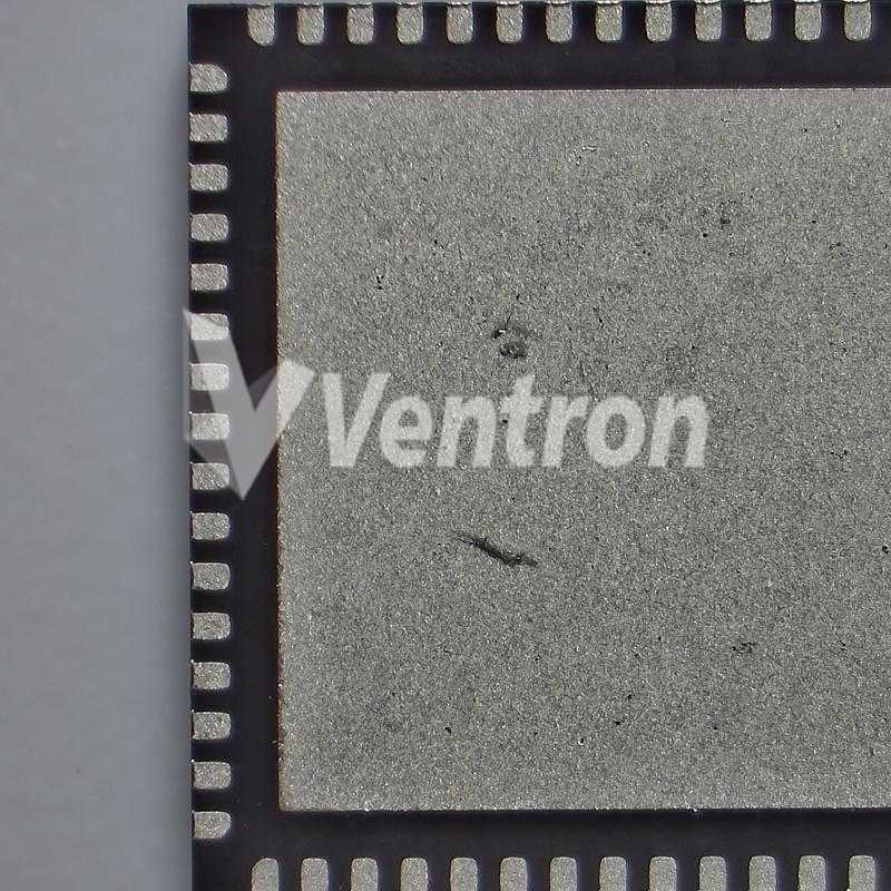
- Package / Case64-WFQFN Exposed Pad
- Number of Pins64
- Operating Temperature-45°C~85°C
- PackagingTape & Reel (TR)
- SeriesPLLatinum™
- JESD-609 Codee3
- Pbfree Codeyes
- Part StatusActive
- Moisture Sensitivity Level (MSL)1 (Unlimited)
- Number of Terminations64
- ECCN CodeEAR99
- Terminal FinishMatte Tin (Sn)
- Voltage - Supply3.15V~3.45V
- Terminal PositionQUAD
- Terminal FormNO LEAD
- Supply Voltage3.3V
- Terminal Pitch0.5mm
- Base Part NumberLMK04208
- OutputLVCMOS, LVDS, LVPECL
- Number of Outputs7
- Number of Circuits1
- uPs/uCs/Peripheral ICs TypeCLOCK GENERATOR, OTHER
- Supply Current-Max535mA
- Frequency (Max)1.536GHz
- Number of Inputs2
- InputLVCMOS, LVDS, LVPECL
- Ratio - Input:Output2:7
- Primary Clock/Crystal Frequency-Nom20.5MHz
- PLLYes
- Differential - Input:OutputYes/Yes
- Divider/MultiplierYes/No
- Height800μm
- Length9mm
- Width9mm
- Thickness0m
- RoHS StatusROHS3 Compliant
- Lead FreeLead Free
The three parts on the right have similar specifications to LMK04208NKDR.
-
ImagePart NumberManufacturerFactory Lead TimeLifecycle StatusMountMounting TypePackage / CaseNumber of PinsOperating TemperaturePackagingSeriesJESD-609 CodePbfree CodePart StatusMoisture Sensitivity Level (MSL)Number of TerminationsECCN CodeTerminal FinishVoltage - SupplyTerminal PositionTerminal FormSupply VoltageTerminal PitchBase Part NumberOutputNumber of OutputsNumber of CircuitsuPs/uCs/Peripheral ICs TypeSupply Current-MaxFrequency (Max)Number of InputsInputRatio - Input:OutputPrimary Clock/Crystal Frequency-NomPLLDifferential - Input:OutputDivider/MultiplierHeightLengthWidthThicknessRoHS StatusLead FreePeak Reflow Temperature (Cel)FrequencyPin CountNominal Supply CurrentPower ConsumptionSubcategoryPacking MethodTechnologyNumber of FunctionsSupply Voltage-Max (Vsup)Power SuppliesMax I(ol)Radiation HardeningView Compare
-
 LMK04208NKDR6 WeeksACTIVE (Last Updated: 5 days ago)Surface MountSurface Mount64-WFQFN Exposed Pad64-45°C~85°CTape & Reel (TR)PLLatinum™e3yesActive1 (Unlimited)64EAR99Matte Tin (Sn)3.15V~3.45VQUADNO LEAD3.3V0.5mmLMK04208LVCMOS, LVDS, LVPECL71CLOCK GENERATOR, OTHER535mA1.536GHz2LVCMOS, LVDS, LVPECL2:720.5MHzYesYes/YesYes/No800μm9mm9mm0mROHS3 CompliantLead Free--------------
 -
6 WeeksACTIVE (Last Updated: 1 day ago)Surface MountSurface Mount48-WFQFN Exposed Pad48-40°C~85°CTape & Reel (TR)-e3yesActive3 (168 Hours)48-Matte Tin (Sn)3.15V~3.45VQUAD-3.3V0.5mmLMK03001LVDS, LVPECL91--1.57GHz-LVCMOS, LVDS, LVPECL1:8800MHzNoYes/YesYes/No800μm7mm7mm750μmROHS3 CompliantLead Free260200MHz4886mA1.18W--------
-
6 WeeksACTIVE (Last Updated: 5 days ago)Surface MountSurface Mount48-WFQFN Exposed Pad48-40°C~85°CTape & Reel (TR)-e3yesActive3 (168 Hours)48EAR99Matte Tin (Sn)3.15V~3.45VQUAD-3.3V0.5mmLMK04001LVCMOS, 2VPECL, LVPECL71--1.57GHz2LVCMOS, LVDS, LVPECL2:7-YesYes/Yes-800μm7mm7mm750μmROHS3 CompliantLead Free260-48--Clock DriversTRBICMOS13.45V3.3V0.0005 ANo
-
6 WeeksACTIVE (Last Updated: 1 week ago)Surface MountSurface Mount48-WFQFN Exposed Pad48-40°C~85°CTape & Reel (TR)-e3yesActive3 (168 Hours)48EAR99Matte Tin (Sn)3.15V~3.45VQUAD-3.3V0.5mmLMK04031LVCMOS, LVDS, 2VPECL, LVPECL61--1.57GHz2LVCMOS, LVDS, LVPECL2:6-YesYes/Yes-800μm7mm7mm750μmROHS3 CompliantLead Free260-48--Clock DriversTRBICMOS13.45V3.3V0.0005 ANo

Popular Search Part Number
Related Keywords
Search Tags
Latest News
-
01 December 2023
KA3525A PWM Controller Symbol, Equivalents, Working Principle and Applications
Ⅰ. What is PWM controller?Ⅱ. Overview of KA3525A PWM controllerⅢ. KA3525A symbol, footprint and pin configurationⅣ. Technical parameters of KA3525AⅤ. How does the KA3525A PWM controller work?Ⅵ. What... -
04 December 2023
TJA1043 CAN Transceiver: Features, Working Modes, Specifications and Applications
Ⅰ. Overview of TJA1043Ⅱ. What are the features of TJA1043 CAN transceiver?Ⅲ. Pin configuration of TJA1043 CAN transceiverⅣ. Working modes of TJA1043 CAN transceiverⅤ. How does the TJA1043... -
04 December 2023
An Overview of L297 Stepper Motor Controller
Ⅰ. What is a stepper motor driver?Ⅱ. Overview of L297Ⅲ. What are the features of L297 stepper motor controller?Ⅳ. Pin configuration of L297 stepper motor controllerⅤ. Structure and... -
05 December 2023
1N4148 Small Signal Switching Diodes Symbol, Working Principle, Packages and Other Details
Ⅰ. Overview of 1N4148Ⅱ. What are the features of 1N4148 diodes?Ⅲ. Symbol, footprint and pin configuration of 1N4148 diodesⅣ. How does the 1N4148 diodes work?Ⅴ. What are the...
Help you to save your cost and time.
Reliable package for your goods.
Fast Reliable Delivery to save time.
Quality premium after-sale service.