
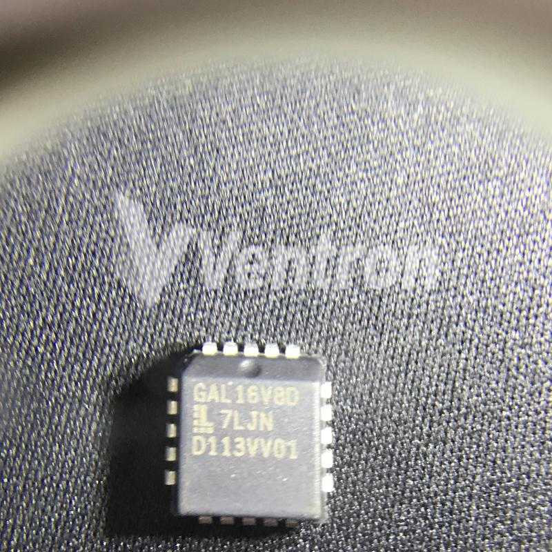
Lattice Semiconductor Corporation GAL16V8D-7LJN
- Part Number:
- GAL16V8D-7LJN
- Manufacturer:
- Lattice Semiconductor Corporation
- Ventron No:
- 3629934-GAL16V8D-7LJN
- Description:
- IC CPLD 8MC 7.5NS 20PLCC
- ECAD Model:
-
- Datasheet:
- GAL16V8
Lattice Semiconductor Corporation GAL16V8D-7LJN technical specifications, attributes, parameters and parts with similar specifications to Lattice Semiconductor Corporation GAL16V8D-7LJN.
- MountSurface Mount
- Mounting TypeSurface Mount
- Package / Case20-LCC (J-Lead)
- Number of Pins20
- Operating Temperature0°C~75°C TA
- PackagingBulk
- Published2000
- SeriesGAL®16V8
- JESD-609 Codee3
- Pbfree Codeyes
- Part StatusObsolete
- Moisture Sensitivity Level (MSL)1 (Unlimited)
- Number of Terminations20
- ECCN CodeEAR99
- Terminal FinishMatte Tin (Sn)
- SubcategoryProgrammable Logic Devices
- TechnologyCMOS
- Terminal PositionQUAD
- Terminal FormJ BEND
- Peak Reflow Temperature (Cel)250
- Supply Voltage5V
- Terminal Pitch1.27mm
- Frequency125MHz
- Reflow Temperature-Max (s)40
- Base Part NumberGAL16V8
- Pin Count20
- Number of Outputs8
- Operating Supply Voltage5V
- Power Supplies5V
- Programmable TypeEE PLD
- Max Supply Voltage5.25V
- Min Supply Voltage4.75V
- Number of I/O8
- Nominal Supply Current115mA
- Max Supply Current115mA
- Propagation Delay7.5 ns
- Turn On Delay Time7.5 ns
- ArchitecturePAL-TYPE
- Number of Inputs16
- Output FunctionMACROCELL
- Number of Macro Cells8
- Number of Dedicated Inputs8
- Voltage Supply - Internal4.75V~5.25V
- Number of Product Terms64
- Height Seated (Max)4.572mm
- Radiation HardeningNo
- REACH SVHCNo SVHC
- RoHS StatusRoHS Compliant
- Lead FreeLead Free
GAL16V8D-7LJN Overview
The mobile phone network has 8 macro cells, which are cells that provide radio coverage from high-power cell sites (towers, antennas, or masts).The item is enclosed in a 20-LCC (J-Lead) package.As a result, it has 8 I/O ports programmed.It is programmed to terminate devices at [0].As the terminal position of this electrical part is [0], it serves as an important access point for passengers or freight.A voltage of 5V is used as the power supply for this device.There is a part in the family [0].As a result, it is packaged as Bulk.In order to ensure the reliability of the device, it is designed to operate at a temperature of [0].It is recommended that the chip be mounted by Surface Mount.The GAL?16V8series FPGA is one of these types.It has 20pins programmed.There are related parts in [0].If high efficiency is desired, the supply voltage should be kept at [0].Surface Mountis used to mount this electronic component.The device is designed with pins [0].A maximum voltage of 5.25Vis required for operation.A minimum supply voltage of 4.75V is required for it to operate.A power supply of 5Vis required to operate it.The frequency that can be achieved is 125MHz.The status of input signals is detected by 8dedicated inputs.The output configuration is set to [0].It is equipped with 64 product terms.16 inputs are employed.A maximal current of 115mAcan be supplied for its operation.
GAL16V8D-7LJN Features
20-LCC (J-Lead) package
8 I/Os
The operating temperature of 0°C~75°C TA
20 pin count
20 pins
5V power supplies
8 outputs
GAL16V8D-7LJN Applications
There are a lot of Lattice Semiconductor Corporation GAL16V8D-7LJN CPLDs applications.
Interface bridging
Address decoders
ROM patching
Digital designs
TIMERS/COUNTERS
High speed graphics processing
Multiple DIP Switch Replacement
Boolean function generators
State machine control
DDC INTERFACE
GAL16V8D-7LJN More Descriptions
Simple Programmable Logic Devices - SPLDs 16 Input, 8 Output 5V, Low Power, 7.5ns
SPLD GAL Family 8 Macro Cells 125MHz 5V 20-Pin PLCC
PLD, 8 MC 125MHZ EECMOS 5V 20 PLCC
Product Description Demo for Development.
EE PLD, 7.5ns, PAL-Type, CMOS, PQCC20
CMOS GAL EEPLD, 16V8, PLCC20, 5V
CMOS GAL EEPLD, 16V8, PLCC20, 5V; Logic Type:EEPLD; Propagation Delay:7.5ns; No. of I/O's:8; Frequency:125MHz; Supply Current Max:115mA; Supply Voltage Range:4.75V to 5.25V; Operating Temperature Range:0°C to 70°C; Logic Case Style:PLCC; No. of Pins:20; SVHC:No SVHC (15-Dec-2010); Base Number:16; I/O Interface Standard:CMOS; IC Generic Number:16V8; IC Temperature Range:Commercial; Logic Function Number:16V8; Logic IC Family:GAL16V8; Logic IC Function:Programmable GAL; No. of Inputs:16; No. of Macrocells:8; Operating Temperature Max:70°C; Operating Temperature Min:0°C; Package / Case:PLCC; Programmable Logic Type:PLD; Supply Voltage:5V; Supply Voltage Max:5.25V; Supply Voltage Min:4.75V; Termination Type:SMD
Popular Search Part Number
Related Keywords
Search Tags
Latest News
-
29 December 2023
An Introduction to HEF4093BP CMOS NAND Schmitt Trigger
Ⅰ. What is HEF4093BP?Ⅱ. Symbol, footprint and 3D model of HEF4093BPⅢ. The specifications of HEF4093BPⅣ. Limiting values of HEF4093BPⅤ. How does HEF4093BP work?Ⅵ. HEF4093BP's market trendⅦ. Where is... -
29 December 2023
TPS54331DR Converter Replacements, Characteristics, Applications and Other Details
Ⅰ. Overview of TPS54331DRⅡ. Characteristics of TPS54331DR converterⅢ. Technical parameters of TPS54331DRⅣ. Typical application of TPS54331DR converterⅤ. Programming the slow start time of TPS54331DRⅥ. Pin configuration of TPS54331DR... -
02 January 2024
STM32F030C8T6 Microcontroller Features, Specifications, Package, Usage and Applications
Ⅰ. What is STM32F030C8T6?Ⅱ. What are the features of STM32F030C8T6?Ⅲ. Specifications of STM32F030C8T6Ⅳ. STM32F030C8T6 Flash reading and writingⅤ. Package of STM32F030C8T6Ⅵ. How to use STM32F030C8T6?Ⅶ. Where is STM32F030C8T6... -
02 January 2024
ADE7953ACPZ Price, Advantages and Disadvantages, Application Fields and More
Ⅰ. ADE7953ACPZ descriptionⅡ. Technical parameters of ADE7953ACPZⅢ. Price and inventory of ADE7953ACPZⅣ. What are the advantages and disadvantages of ADE7953ACPZ?Ⅴ. Circuit diagram of ADE7953ACPZⅥ. How does ADE7953ACPZ achieve...

Help you to save your cost and time.
Reliable package for your goods.
Fast Reliable Delivery to save time.
Quality premium after-sale service.