
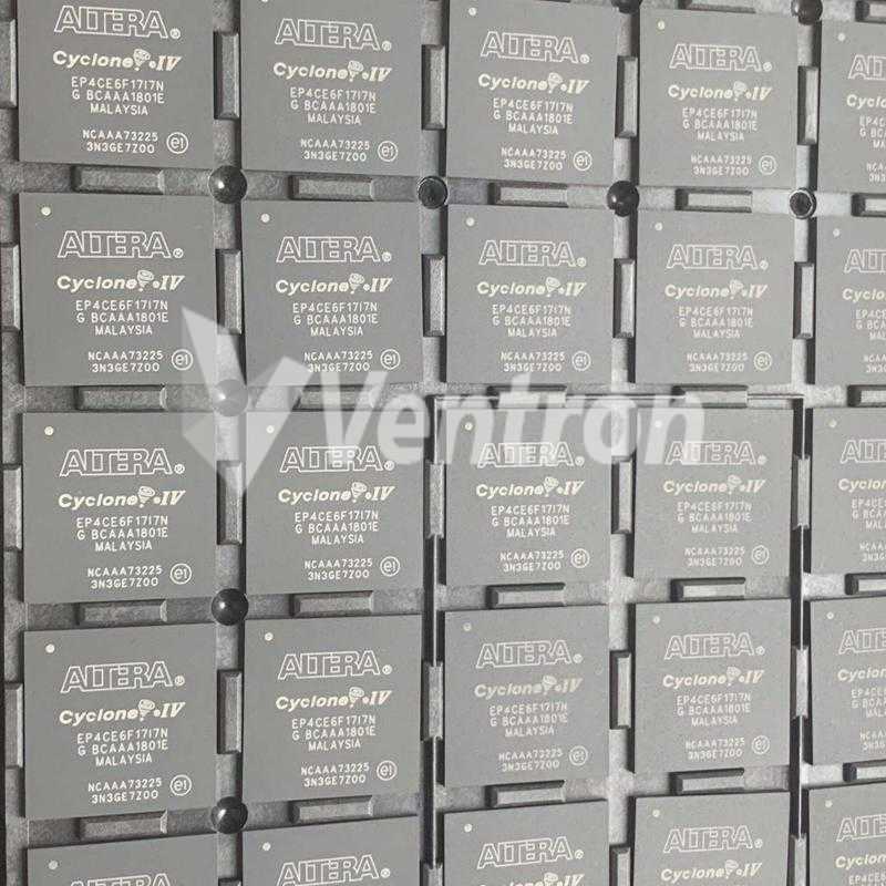
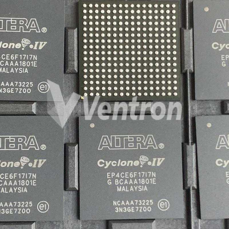
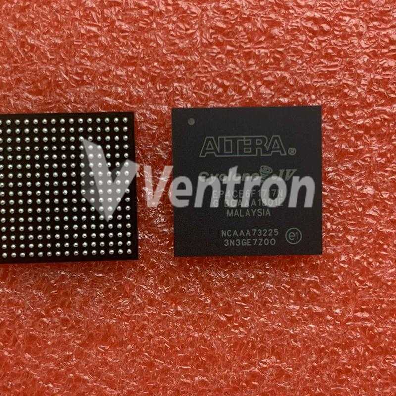
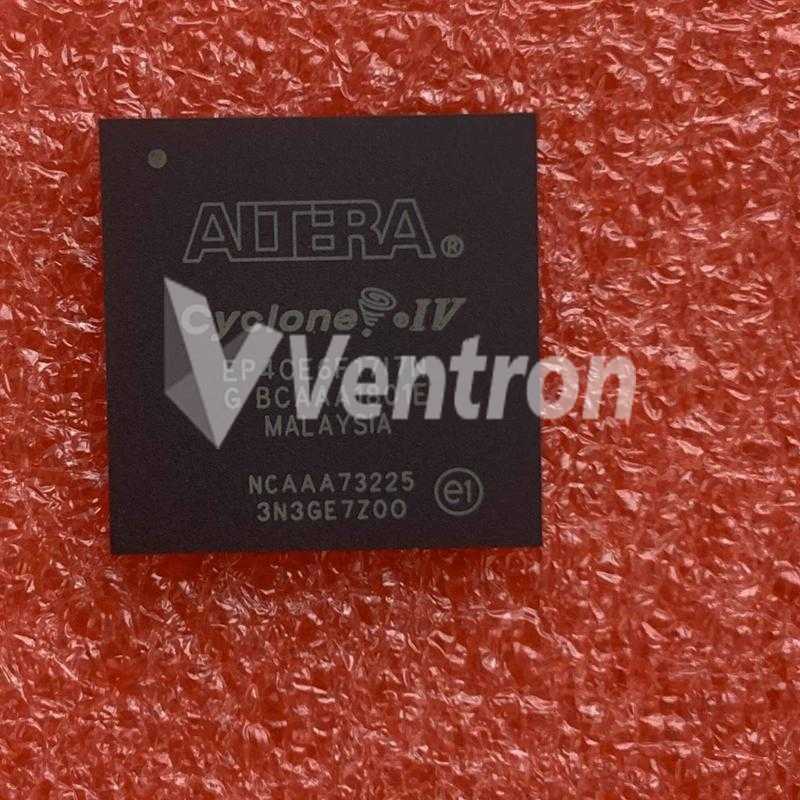
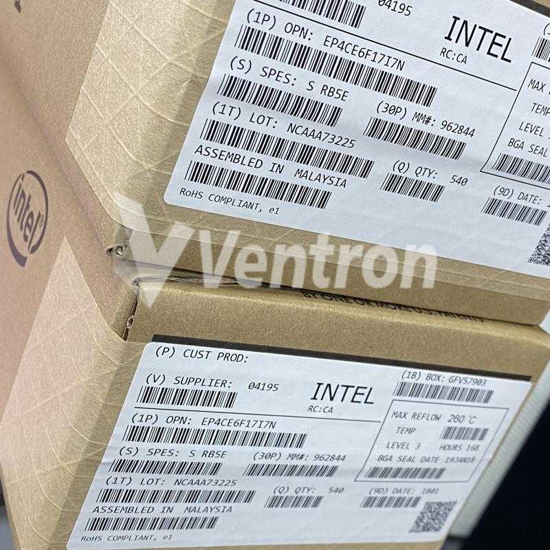
Altera EP4CE6F17I7N
- Part Number:
- EP4CE6F17I7N
- Manufacturer:
- Altera
- Ventron No:
- 3125726-EP4CE6F17I7N
- Description:
- IC FPGA 179 I/O 256FBGA
- ECAD Model:
-
- Datasheet:
- Cyclone IV Device Handbook


Altera EP4CE6F17I7N technical specifications, attributes, parameters and parts with similar specifications to Altera EP4CE6F17I7N.
- Factory Lead Time8 Weeks
- Mounting TypeSurface Mount
- Package / Case256-LBGA
- Surface MountYES
- Operating Temperature-40°C~100°C TJ
- PackagingTray
- Published2016
- SeriesCyclone® IV E
- JESD-609 Codee1
- Part StatusActive
- Moisture Sensitivity Level (MSL)3 (168 Hours)
- Number of Terminations256
- Terminal FinishTin/Silver/Copper (Sn/Ag/Cu)
- HTS Code8542.39.00.01
- SubcategoryField Programmable Gate Arrays
- Voltage - Supply1.15V~1.25V
- Terminal PositionBOTTOM
- Terminal FormBALL
- Peak Reflow Temperature (Cel)260
- Supply Voltage1.2V
- Terminal Pitch1mm
- Reflow Temperature-Max (s)40
- Base Part NumberEP4CE6
- JESD-30 CodeS-PBGA-B256
- Number of Outputs179
- Qualification StatusNot Qualified
- Power Supplies1.21.2/3.32.5V
- Number of I/O179
- Clock Frequency472.5MHz
- Number of Inputs179
- Programmable Logic TypeFIELD PROGRAMMABLE GATE ARRAY
- Number of Logic Elements/Cells6272
- Total RAM Bits276480
- Number of LABs/CLBs392
- Number of CLBs392
- Height Seated (Max)2.2mm
- Length17mm
- Width17mm
- RoHS StatusRoHS Compliant
EP4CE6F17I7N Overview
There are two packages that contain fpga chips: 256-LBGA package and X package. FPGAs of this type consist of FIELD PROGRAMMABLE GATE ARRAY components. A total of 179 I/Os are programmed to ensure a more coherent data transfer. A fundamental building block contains 6272 logic elements or cells. Fpga chips is powered from a supply voltage of 1.2V. Field Programmable Gate Arrays family FPGA part. Using a Surface Mount connector, you can mount this FPGA module on the development board. The supply voltage of the device is 1.15V~1.25V , at which it runs. This is a type of FPGA that is part of the Cyclone? IV E series of FPGAs. As far as the operating temperature is concerned, it should be kept within -40°C~100°C TJ when operating. This device is equipped with 179 separate outputs, which makes it a very versatile device. In order to save space, this FPGA model has been contained in Tray. Total terminations are 256. Fpga chips is important to note that this device has a RAM capacFpga chipsy of 276480 bFpga chipss. In order to find related parts, use the part number EP4CE6 as a base. The FPGA consists of 392 LABs/CLBs. Power is supplied to the device by a 1.21.2/3.32.5V battery. Most of the time, it uses a crystal oscillating at 472.5MHz to generate the signal. The architecture of the system is based on 392 CLBs.
EP4CE6F17I7N Features
179 I/Os
Up to 276480 RAM bits
EP4CE6F17I7N Applications
There are a lot of Intel EP4CE6F17I7N FPGAs applications.
Computer hardware emulation
Enterprise networking
Space Applications
Automotive driver's assistance
Radar and Sensors
Embedded Vision
Industrial IoT
Medical Electronics
Voice recognition
Device controllers
EP4CE6F17I7N More Descriptions
FPGA Cyclone® IV E Family 6272 Cells 60nm Technology 1.2V 256-Pin TFBGA
Field Programmable Gate Array, 392 CLBs, 472.5MHz, 6272-Cell, PBGA256
6272 392 BGA-256 Programmable Logic Device (CPLDs/FPGAs) ROHS
2003 RoHS Compliant BALL Not Qualified FPGA 100C 33.8kB 200MHz 1.24V
IC FPGA 179 I/O 256FBGA Cyclone IV E
IC,FPGA,EP4CE6,179I/O,CYCLON IV,FBGA-256
6272LogC 392LABs 179I/O BGA256
Product Description Demo for Development.
IC DAC 16BIT QUAD MULT 28-SSOP
French Electronic Distributor since 1988
Field Programmable Gate Arrays
The three parts on the right have similar specifications to EP4CE6F17I7N.
-
ImagePart NumberManufacturerFactory Lead TimeMounting TypePackage / CaseSurface MountOperating TemperaturePackagingPublishedSeriesJESD-609 CodePart StatusMoisture Sensitivity Level (MSL)Number of TerminationsTerminal FinishHTS CodeSubcategoryVoltage - SupplyTerminal PositionTerminal FormPeak Reflow Temperature (Cel)Supply VoltageTerminal PitchReflow Temperature-Max (s)Base Part NumberJESD-30 CodeNumber of OutputsQualification StatusPower SuppliesNumber of I/OClock FrequencyNumber of InputsProgrammable Logic TypeNumber of Logic Elements/CellsTotal RAM BitsNumber of LABs/CLBsNumber of CLBsHeight Seated (Max)LengthWidthRoHS StatusECCN CodeView Compare
-
 EP4CE6F17I7N8 WeeksSurface Mount256-LBGAYES-40°C~100°C TJTray2016Cyclone® IV Ee1Active3 (168 Hours)256Tin/Silver/Copper (Sn/Ag/Cu)8542.39.00.01Field Programmable Gate Arrays1.15V~1.25VBOTTOMBALL2601.2V1mm40EP4CE6S-PBGA-B256179Not Qualified1.21.2/3.32.5V179472.5MHz179FIELD PROGRAMMABLE GATE ARRAY62722764803923922.2mm17mm17mmRoHS Compliant--
 -
8 WeeksSurface Mount484-BGAYES-40°C~100°C TJTray-Cyclone® IV Ee0Active3 (168 Hours)484Tin/Lead (Sn/Pb)8542.39.00.01Field Programmable Gate Arrays1.15V~1.25VBOTTOMBALL2201.2V1mm30EP4CE115S-PBGA-B484283Not Qualified1.21.2/3.32.5V280472.5MHz283FIELD PROGRAMMABLE GATE ARRAY11448039813127155-2.4mm23mm23mmNon-RoHS Compliant3A001.A.7.A
-
8 WeeksSurface Mount256-LBGAYES-40°C~100°C TJTray2016Cyclone® IV Ee0Active3 (168 Hours)256TIN LEAD8542.39.00.01Field Programmable Gate Arrays1.15V~1.25VBOTTOMBALL2201.2V1mm30EP4CE10S-PBGA-B256179Not Qualified1.21.2/3.32.5V179472.5MHz179FIELD PROGRAMMABLE GATE ARRAY103204239366456451.55mm17mm17mmNon-RoHS Compliant-
-
11 WeeksSurface Mount144-LQFP Exposed PadYES0°C~85°C TJTray2016Cyclone® IV Ee3Active3 (168 Hours)144MATTE TIN (472) OVER COPPER8542.39.00.01Field Programmable Gate Arrays1.15V~1.25VQUADGULL WING2601.2V0.5mm40EP4CE10S-PQFP-G14491Not Qualified1.21.2/3.32.5V91472.5MHz91FIELD PROGRAMMABLE GATE ARRAY103204239366456451.65mm20mm20mmRoHS Compliant-

Popular Search Part Number
Related Keywords
Search Tags
Latest News
-
08 November 2023
What is MOC3021 Optocoupler Triac Driver?
Ⅰ. What is an optocoupler?Ⅱ. Overview of MOC3021 optocouplerⅢ. Pin configuration of MOC3021 optocouplerⅣ. Features of MOC3021 optocouplerⅤ. Technical parameters of MOC3021 optocouplerⅥ. Working principle of MOC3021 optocouplerⅦ.... -
08 November 2023
LM324 vs LM358: What is the Difference Between Them?
Ⅰ. What is an operational amplifier?Ⅱ. Overview of LM324Ⅲ. Overview of LM358Ⅳ. LM324 vs LM358: FeaturesⅤ. LM324 vs LM358: Technical parametersⅥ. LM324 vs LM358: Pin configurationⅦ. LM324 vs... -
09 November 2023
TL3845P PWM Controller: Symbol, Features and Layout Guidelines
Ⅰ. What is a PWM controller?Ⅱ. Overview of TL3845P PWM controllerⅢ. Symbol, footprint and pin configuration of TL3845PⅣ. Features of TL3845P PWM controllerⅤ. Technical parameters of TL3845P PWM... -
09 November 2023
2N3904 NPN Transistor: Equivalents, Manufacturer, Working Principle and Applications
Ⅰ. Overview of 2N3904 transistorⅡ. Manufacturer of 2N3904 transistorⅢ. Symbol, footprint and pin configuration of 2N3904 transistorⅣ. What are the features of 2N3904 transistor?Ⅴ. Technical parameters of 2N3904...
Help you to save your cost and time.
Reliable package for your goods.
Fast Reliable Delivery to save time.
Quality premium after-sale service.