Microsemi Corporation AX500-2FGG676I
- Part Number:
- AX500-2FGG676I
- Manufacturer:
- Microsemi Corporation
- Ventron No:
- 3635007-AX500-2FGG676I
- Description:
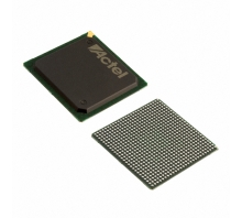
- IC FPGA 336 I/O 676FBGA
- ECAD Model:
-
- Datasheet:
- AX500-2FGG676I
Microsemi Corporation AX500-2FGG676I technical specifications, attributes, parameters and parts with similar specifications to Microsemi Corporation AX500-2FGG676I.
- Factory Lead Time16 Weeks
- Lifecycle StatusIN PRODUCTION (Last Updated: 4 weeks ago)
- MountSurface Mount
- Mounting TypeSurface Mount
- Package / Case676-BGA
- Number of Pins676
- Weight400.011771mg
- Operating Temperature-40°C~85°C TA
- PackagingTray
- Published2012
- SeriesAxcelerator
- JESD-609 Codee1
- Part StatusActive
- Moisture Sensitivity Level (MSL)3 (168 Hours)
- Number of Terminations676
- Terminal FinishTin/Silver/Copper (Sn/Ag/Cu)
- SubcategoryField Programmable Gate Arrays
- TechnologyCMOS
- Voltage - Supply1.425V~1.575V
- Terminal PositionBOTTOM
- Terminal FormBALL
- Peak Reflow Temperature (Cel)250
- Supply Voltage1.5V
- Terminal Pitch1mm
- Frequency870MHz
- Reflow Temperature-Max (s)40
- Base Part NumberAX500
- Number of Outputs336
- Operating Supply Voltage1.5V
- Number of I/O336
- RAM Size9kB
- Propagation Delay740 ps
- Turn On Delay Time740 ps
- Programmable Logic TypeFIELD PROGRAMMABLE GATE ARRAY
- Total RAM Bits73728
- Number of Gates500000
- Number of LABs/CLBs8064
- Speed Grade2
- Number of Registers5376
- Combinatorial Delay of a CLB-Max0.74 ns
- Height1.73mm
- Length27mm
- Width27mm
- Radiation HardeningNo
- RoHS StatusRoHS Compliant
AX500-2FGG676I Overview
Microsemi Corporation offers a highly advanced Embedded - FPGAs (Field Programmable Gate Array) chip, designed for efficient and versatile performance. This chip falls under the Embedded - FPGAs (Field Programmable Gate Array) category and comes in a 676-BGA package. It is packaged in a tray and operates at a voltage supply of 1.425V~1.575V. With 336 outputs and an operating supply voltage of 1.5V, this chip also boasts a RAM size of 9kB and a total RAM bits of 73728. The propagation delay for this chip is 740 ps and the combinatorial delay of a CLB-Max is 0.74 ns. Additionally, it has a height of 1.73mm, making it a compact and powerful option for various applications.
AX500-2FGG676I Features
336 I/Os
Up to 73728 RAM bits
676 LABs/CLBs
5376 registers
Operating from a frequency of 870MHz
AX500-2FGG676I Applications
There are a lot of Microsemi Corporation AX500-2FGG676I FPGAs applications.
Automotive driver's assistance
Automotive Applications
Audio
Solar Energy
Video & Image Processing
Automotive
Distributed Monetary Systems
Wired Communications
Secure Communication
Industrial,Medical and Scientific Instruments
AX500-2FGG676I More Descriptions
FPGA Axcelerator Family 286K Gates 5376 Cells 870MHz 0.15um (CMOS) Technology 1.5V 676-Pin FBGA
Axcelerator FPGA 500K System Gates
IC FPGA 336 I/O 676FBGA
Axcelerator FPGA 500K System Gates
IC FPGA 336 I/O 676FBGA

Popular Search Part Number
Related Keywords
Search Tags
Latest News
-
26 October 2023
L293DNE Quadruple Half-H Driver: Symbol, Features, Advantages and More
Ⅰ. Overview of L293DNE quadruple half-H driverⅡ. L293DNE symbol, footprint and pin configurationⅢ. Technical parameters of L293DNE/aⅣ. What are the features of L293DNE?Ⅴ. Working principle of L293DNEⅥ. What... -
26 October 2023
TL494CN PWM Controller: Pin Configuration, Layout Guidelines and Working Principle
Ⅰ. Overview of TL494CN PWM controllerⅡ. Symbol, footprint and pin configuration of TL494CN PWM controllerⅢ. Technical parameters of TL494CN PWM controllerⅣ. What are the features of TL494CN PWM... -
27 October 2023
CD4511BE Decoder: Pin Configuration, Features, Circuit and Applications
Ⅰ. What is a decoder?Ⅱ. Overview of CD4511BE decoderⅢ. Symbol, footprint and pin configuration of CD4511BE decoderⅣ. Technical parameters of CD4511BE decoderⅤ. What are the features of CD4511BE... -
27 October 2023
A Complete Guide to The BC639 BJT Transistor
Ⅰ. Overview of BC639 transistorⅡ. BC639 transistor symbol, footprint and pin configurationⅢ. Technical parameters of BC639 transistorⅣ. Characteristics of BC639 transistorⅤ. Working principle of BC639 transistorⅥ. Maximum ratings...

Help you to save your cost and time.
Reliable package for your goods.
Fast Reliable Delivery to save time.
Quality premium after-sale service.