
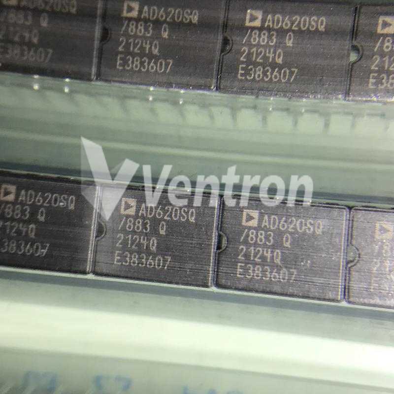
Analog Devices Inc. AD620BN
- Part Number:
- AD620BN
- Manufacturer:
- Analog Devices Inc.
- Ventron No:
- 3696467-AD620BN
- Description:
- IC OPAMP INSTR 1MHZ 8DIP
- ECAD Model:
-
- Datasheet:
- AD620BN

Analog Devices Inc. AD620BN technical specifications, attributes, parameters and parts with similar specifications to Analog Devices Inc. AD620BN.
- Contact PlatingLead, Tin
- MountThrough Hole
- Mounting TypeThrough Hole
- Package / Case8-DIP (0.300, 7.62mm)
- Number of Pins8
- Operating Temperature-40°C~85°C
- PackagingTube
- JESD-609 Codee0
- Pbfree Codeno
- Part StatusObsolete
- Moisture Sensitivity Level (MSL)1 (Unlimited)
- Number of Terminations8
- ECCN CodeEAR99
- Resistance10GOhm
- Max Power Dissipation650mW
- Terminal PositionDUAL
- Number of Functions1
- Supply Voltage15V
- Terminal Pitch2.54mm
- Base Part NumberAD620
- Pin Count8
- Operating Supply Voltage36V
- Number of Elements1
- Operating Supply Current1.3mA
- Nominal Supply Current1.3mA
- Power Dissipation650mW
- Slew Rate1.2V/μs
- Amplifier TypeInstrumentation
- Common Mode Rejection Ratio93 dB
- Current - Input Bias500pA
- Voltage - Supply, Single/Dual (±)4.6V~36V ±2.3V~18V
- Output Current per Channel18mA
- Input Offset Voltage (Vos)30mV
- Neg Supply Voltage-Nom (Vsup)-15V
- Voltage - Input Offset15μV
- 3db Bandwidth1MHz
- Input Offset Current-Max (IIO)0.00075μA
- Voltage Gain-Min1
- Voltage Gain-Nom10
- Non-linearity-Max0.004%
- Height Seated (Max)4.57mm
- Length9.27mm
- Radiation HardeningNo
- RoHS StatusNon-RoHS Compliant
- Lead FreeContains Lead
AD620BN Overview
The brand of this particular component is Analog Devices Inc. It falls under the category of Linear - Amplifiers - Instrumentation, OP Amps, Buffer Amps. The contact plating material used for this chip is Lead and Tin. It is designed for through-hole mounting and the package or case type is 8-DIP (0.300, 7.62mm). The JESD-609 Code assigned to this chip is e0. The terminal pitch, which refers to the distance between the center of one terminal to the center of the adjacent terminal, is 2.54mm. The operating supply voltage for this chip is 36V. The negative supply voltage, also known as Vsup, is -15V. The voltage gain, which is the ratio of the output voltage to the input voltage, is 10. Lastly, it is important to note that this chip is not compliant with the RoHS (Restriction of Hazardous Substances) directive.
AD620BN Features
8 Pins
supply voltage of 15V
Resistance of 10GOhm
AD620BN Applications
There are a lot of Analog Devices Inc. AD620BN Instrumentational OP Amps applications.
Weighing systems
Measurements of Wheatstone bridge
Fission chambers
Multimedia playback equipment
Automation control systems
Home audio systems
Portable media players
Exponential operation circuits
Television
Active probe
AD620BN More Descriptions
Low Cost, Low Power Instrumentation Amplifier | IC INST AMP 1 CIRCUIT 8DIP
Instrumentation Amplifier, 1 Func, 85uV Offset-Max, 1MHz Band Width, PDIP8
The AD620 is a low cost, high accuracy instrumentation amplifier that requires only one external resistor to set gains of 1 to 10,000. Furthermore, the AD620 features 8-lead SOIC and DIP packaging that is smaller than discrete designs and offers lower power (only 1.3 mA max supply current), making it a good fit for battery powered, portable (or remote) applications. The AD620, with its high accuracy of 40 ppm maximum nonlinearity, low offset voltage of 50 µV max, and offset drift of 0.6 µV/°C max, is ideal for use in precision data acquisition systems, such as weigh scales and transducer interfaces. Furthermore, the low noise, low input bias current, and low power of the AD620 make it well suited for medical applications such as ECG and noninvasive blood pressure monitors. The low input bias current of 1.0 nA max is made possible with the use of Superϐeta processing in the input stage. The AD620 works well as a preamplifier due to its low input voltage noise of 9 nV/√Hz at 1 kHz, 0.28 μV p-p in the 0.1 Hz to 10 Hz band, and 0.1 pA/√Hz input current noise. Also, the AD620 is well suited for multiplexed applications with its settling time of 15 μs to 0.01%, and its cost is low enough to enable designs with one in-amp per channel.
The three parts on the right have similar specifications to AD620BN.
-
ImagePart NumberManufacturerContact PlatingMountMounting TypePackage / CaseNumber of PinsOperating TemperaturePackagingJESD-609 CodePbfree CodePart StatusMoisture Sensitivity Level (MSL)Number of TerminationsECCN CodeResistanceMax Power DissipationTerminal PositionNumber of FunctionsSupply VoltageTerminal PitchBase Part NumberPin CountOperating Supply VoltageNumber of ElementsOperating Supply CurrentNominal Supply CurrentPower DissipationSlew RateAmplifier TypeCommon Mode Rejection RatioCurrent - Input BiasVoltage - Supply, Single/Dual (±)Output Current per ChannelInput Offset Voltage (Vos)Neg Supply Voltage-Nom (Vsup)Voltage - Input Offset3db BandwidthInput Offset Current-Max (IIO)Voltage Gain-MinVoltage Gain-NomNon-linearity-MaxHeight Seated (Max)LengthRadiation HardeningRoHS StatusLead FreeFactory Lead TimeLifecycle StatusNumber of ChannelsBandwidthGain Bandwidth ProductPower Supply Rejection Ratio (PSRR)Dual Supply VoltageHeightWidthREACH SVHCTechnologyTerminal FormPeak Reflow Temperature (Cel)Reflow Temperature-Max (s)Qualification StatusNumber of CircuitsInput Voltage Noise DensitySurface MountTerminal FinishReach Compliance CodeTime@Peak Reflow Temperature-Max (s)JESD-30 CodeCurrent - SupplyAverage Bias Current-Max (IIB)Current - Output / ChannelView Compare
-
 AD620BNLead, TinThrough HoleThrough Hole8-DIP (0.300, 7.62mm)8-40°C~85°CTubee0noObsolete1 (Unlimited)8EAR9910GOhm650mWDUAL115V2.54mmAD620836V11.3mA1.3mA650mW1.2V/μsInstrumentation93 dB500pA4.6V~36V ±2.3V~18V18mA30mV-15V15μV1MHz0.00075μA1100.004%4.57mm9.27mmNoNon-RoHS CompliantContains Lead--------------------------
 -
TinThrough HoleThrough Hole8-DIP (0.300, 7.62mm)8-40°C~85°CTubee3noActive1 (Unlimited)8EAR9910GOhm650mWDUAL115V2.54mmAD6208--1.3mA900μA650mW1.2V/μsInstrumentation93 dB500pA4.6V~36V ±2.3V~18V18mA30mV-15V15μV1MHz0.00075μA1100.004%-9.27mmNoROHS3 CompliantContains Lead8 WeeksPRODUCTION (Last Updated: 1 month ago)1120 kHz120 kHz140dB9V3.3mm6.35mmNo SVHC---------------
-
TinSurface MountSurface Mount8-SOIC (0.154, 3.90mm Width)8-40°C~85°CTape & Reel (TR)e3noActive1 (Unlimited)8EAR9910GOhm650mWDUAL115V-AD6218-31.3mA-650mW1.2V/μsInstrumentation93 dB500pA±2.3V~18V18mA35μV-15V50μV800kHz0.00075μA10100-2.59mm4.9mm-ROHS3 CompliantContains Lead14 WeeksPRODUCTION (Last Updated: 3 weeks ago)---95dB----BIPOLARGULL WING26030Not Qualified113nV/sqrt Hz--------
-
--Surface Mount8-SOIC (0.154, 3.90mm Width)--40°C~85°CTape & Reel (TR)e0noObsolete1 (Unlimited)8---DUAL115V--8-----1.2V/μsInstrumentation-500pA±2.3V~18V---15V75μV800kHz-10100-2.59mm4.9mm-Non-RoHS Compliant------------GULL WING240-COMMERCIAL1-YESTIN LEADunknown30R-PDSO-G8900μA0.0025μA18mA
Popular Search Part Number
Related Keywords
Search Tags
Latest News
-
16 April 2024
XTR111AIDGQR Alternatives, Pinout, Advantages and Working Principle
Ⅰ. What is XTR111AIDGQR?Ⅱ. XTR111AIDGQR pin diagram and descriptionⅢ. XTR111AIDGQR's external current limitⅣ. XTR111AIDGQR technical advantagesⅤ. Schematic diagram and working principle of XTR111AIDGQRⅥ. Application areas of XTR111AIDGQRⅦ. How... -
16 April 2024
All You Need to Know About the 74HC165 Eight-Bit Shift Register
Ⅰ. Introduction to 74HC165Ⅱ. Functions of 74HC165Ⅲ. Logic diagram of 74HC165Ⅳ. Working principle of 74HC165Ⅴ. Recommended operating conditions of 74HC165Ⅵ. Precautions for using 74HC165Ⅶ. What is the role... -
17 April 2024
TPS5450DDAR: High Performance Step-Down Switching Regulator
Ⅰ. Overview of TPS5450DDARⅡ. Technical parameters of TPS5450DDARⅢ. Simplified schematic of TPS5450DDARⅣ. Features and advantages of TPS5450DDARⅤ. How to configure the soft start function of TPS5450DDAR?Ⅵ. Concrete applications... -
17 April 2024
SI2302 Field Effect Transistor Characteristics, Use and Application Prospects
Ⅰ. Introduction to SI2302Ⅱ. Main characteristics of SI2302Ⅲ. SI2302 driving methodⅣ. Maximum ratings of SI2302Ⅴ. Tips for using SI2302Ⅵ. What can be used to replace SI2302?Ⅶ. Precautions for...
Help you to save your cost and time.
Reliable package for your goods.
Fast Reliable Delivery to save time.
Quality premium after-sale service.